| home | builders | Search |
| builders ➜ TARPN Kits and Projects ➜ NinoTNC N9600A ➜ N9600A4r3 Assembly |
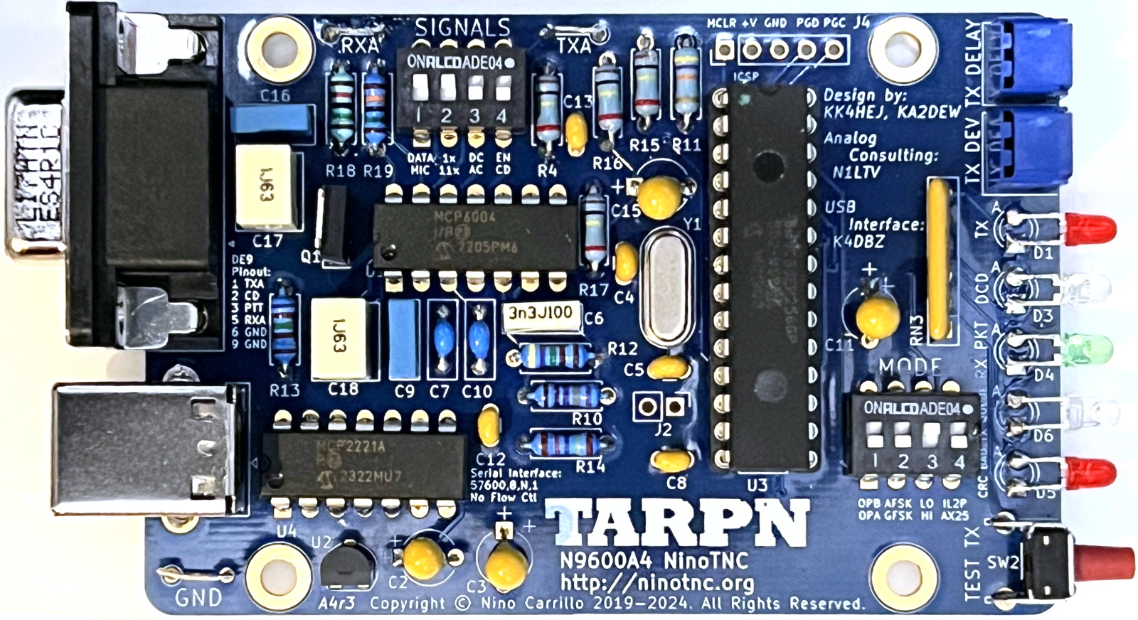
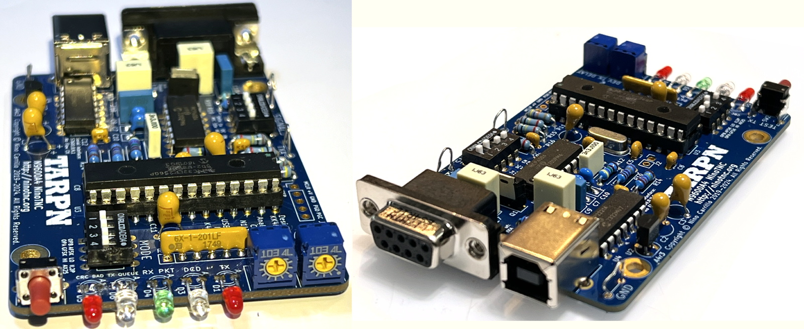
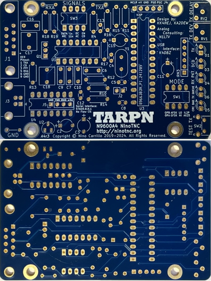
| These are the assembly instructions for the N9600A4r3 blue-board. Make sure the silkscreen information on the board you are assembling matches this. The bill of materials linked below is specific to the A4r3 board which will ship starting in February 2025. |
|
For assembly of the A4RC10, A4r1 and A4r2, see the A4r2 assembly instructions here.
See our History Page for other version information. |
| Bill Of Materials |
Right-click on this link and save the n9600a4r3 p008 bom XLSX spreadsheet file to your computer.
This is the Mouser shopping list for the NinoTNC. Find the n9600a4r3 XLSX file on your computer (it will be named starting with n9600a4r3 and will be a XLSX, Excel Spreadsheet, file) |
|
| Go to Mouser website | Click on this link: Mouser. You might as well register at Mouser because they're going to get your delivery information and whatnot anyway. Registering and logging-in means that your shopping cart is retained through separate sessions, on separate computers, and they will provide you with a history of your orders. |
|
| Shopping Cart | Click on the shopping cart. If there are already items in your cart, you can click on View cart and then New Cart. |
|
| Upload Spreadsheet |
There is an Upload A Spreadsheet field in the middle of the form.
Drag the XLSX file from your Finder/Explorer into that field, or click on Browse your files, and then navigate to the XLSX file. |
|
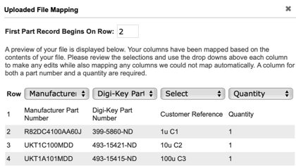
| Price Availability Assistant |
The web page will now want you to specify what the columns in the spreadsheet represent.
By adjusting the drop-down menus at the top of each column, you can tell Mouser that you have Mouser OR Mfr. #, then Qty. 1, then Customer #, and then leave the rest of the field headings blank. The Line items begin on row# should be set to 2. Click on Next |
|
| Mouser may offer that there are multiple parts matching the supplied part number. Find the lowest price in-stock item in the match list and click on Match. | ||
| Save money | if you are ordering parts for more than a single TNC, please be sure to check for quantity discounts. Sometimes ordering 10 is significantly cheaper than ordering eight of something. Price breaks usually start at 10, but sometimes other numbers. | |
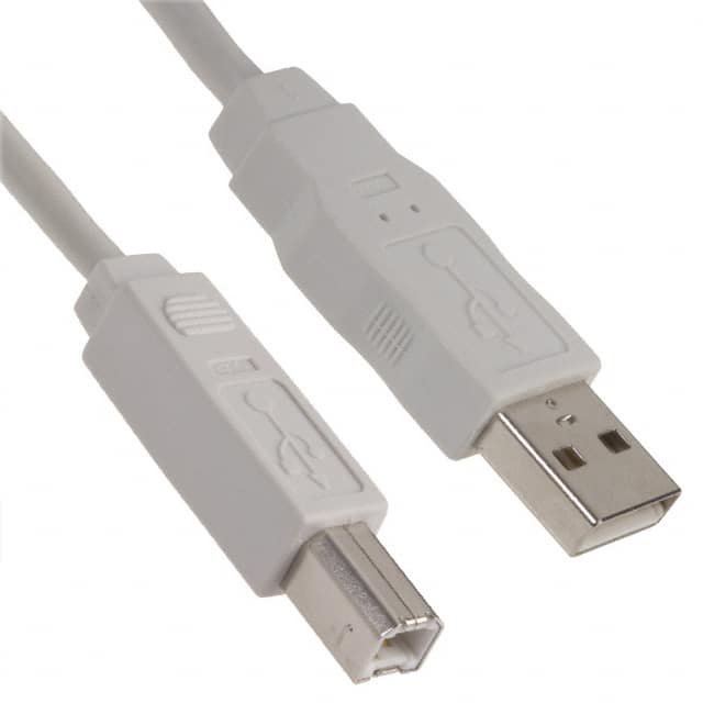
| USB cable? |
If you need a USB A male to USB B printer cable, better shop someplace else as Mouser doesn't seem to be the cheap place to go.
You should be able to find a half-meter printer cable (1 foot or so) for under $5.
In quantity I've gotten them for 50 cents on eBay.
Short is better for RF immunity but it does have to make it from the host computer (Raspberry Pi) to the NinoTNC. |
|
| Checkout |
Inspect the list
1 Ships Now or something like that means good. If anything is On Order, stop and send an email to [email protected] email reflector. Make your subject line the word "BACKORDER" the reference designator, and the BOM filename: For Instance: SUBJECT: BACKORDERED C7 in n9600a4f_bom_p426 Almost everything is available with a different part number or manufacturer right on Mouser. We'll fix the BOM and send you (and the group) a reply. If you go ahead and let it be backorded, Mouser would ship you part of your order, and then when the backordered part is available, they will ship the rest. They may charge you postage twice, or delay your shipment. If everything is available, do checkout and pay for your order. |

|
| ⇒ All parts are inserted from the silk-screened side of the board, i.e. from the side on which the white writing is printed. |
| ⇒ Except where specifically noted, all two pin components are non-polorized so you can put the part onto the board with the pins in either hole. |
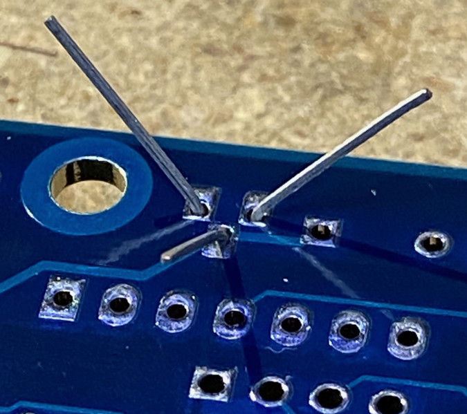 Inspect the leads to make sure the solder comes up over the lead for a visible amount.
Cut the lead at the point where the lead meets the solder, but don't cut the solder.
The solder is your friend.
What you do NOT want is a lead which is not making good electrical contact with the hole.
Inspect the leads to make sure the solder comes up over the lead for a visible amount.
Cut the lead at the point where the lead meets the solder, but don't cut the solder.
The solder is your friend.
What you do NOT want is a lead which is not making good electrical contact with the hole.

 The ground plane and power plane on our printed circuit board (PCB) are not visible on the top and bottom becuase this is a four layer board.
The ground and power are pretty much everywhere except near where wires pass through.
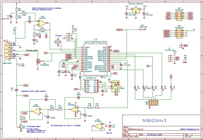
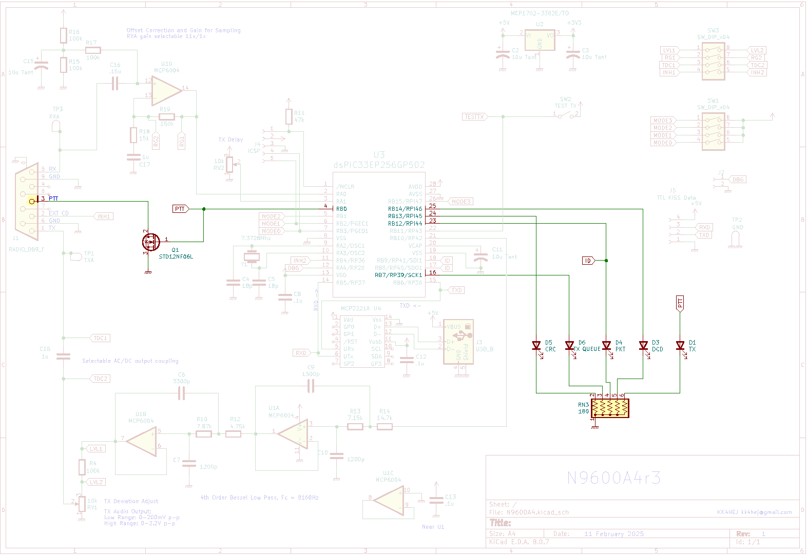
Here's the NinoTNC A4r3 schematic.
Click to load the PDF.
The ground plane and power plane on our printed circuit board (PCB) are not visible on the top and bottom becuase this is a four layer board.
The ground and power are pretty much everywhere except near where wires pass through.
Here's the NinoTNC A4r3 schematic.
Click to load the PDF.
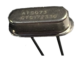
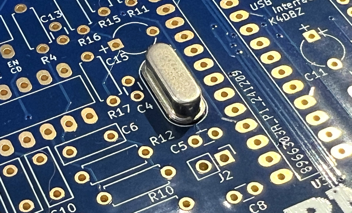
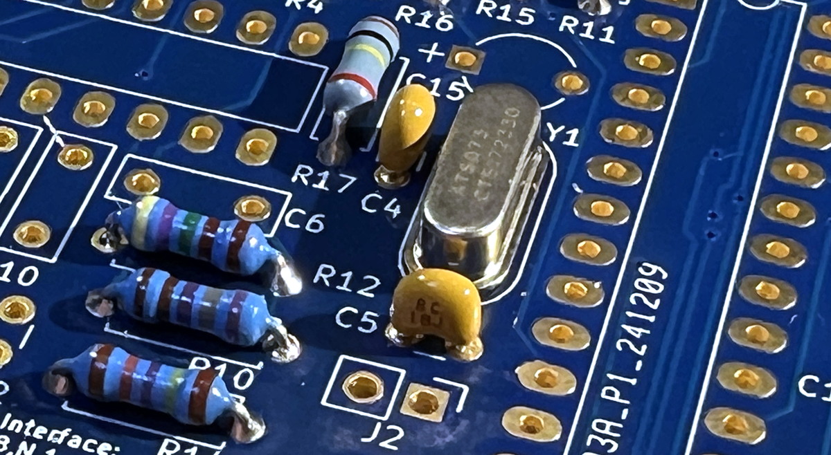
| 1 | Y1 | 7.3728 MHz crystal
|
The crystal will have some lettering on it containing 7 and 3, in order.
It may say 037 or 7.37 or something like that.
The crystal and two capacitors, C4 and C5, form an oscillator to provide clocking for the CPU's digital circuits. 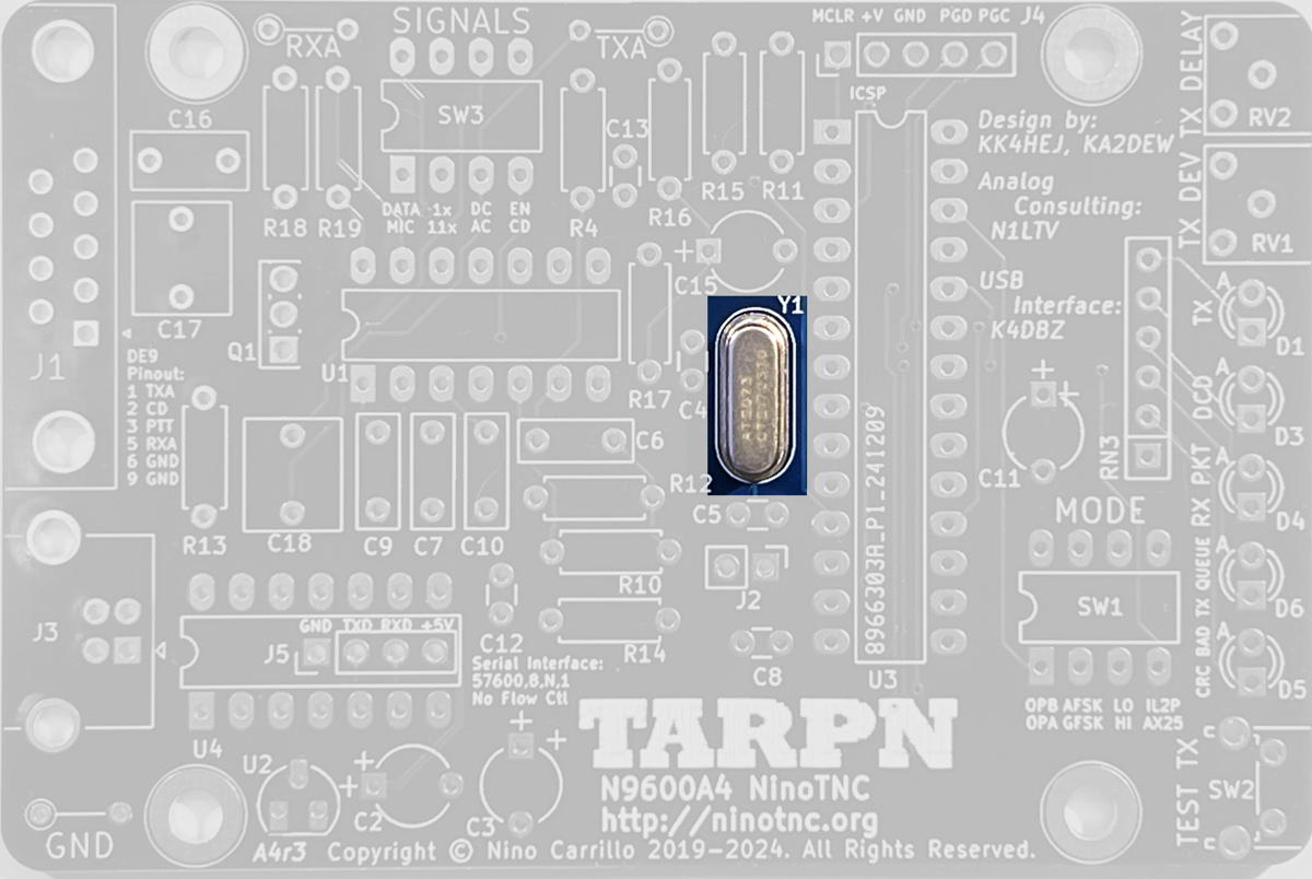
 Schematic showing Y1 and the oscillator circuit:
(click to embiggen)
Schematic showing Y1 and the oscillator circuit:
(click to embiggen)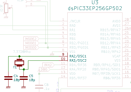
|
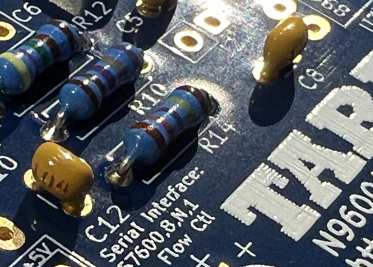
| We have received resistors with two different body colors. The stripes, indicating the resistor value, have been correct and the same for the different manufacture or batch, but the body of the resistor has been beige or blue. |
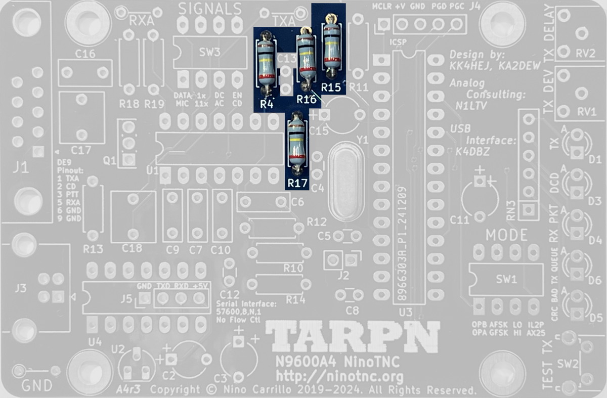
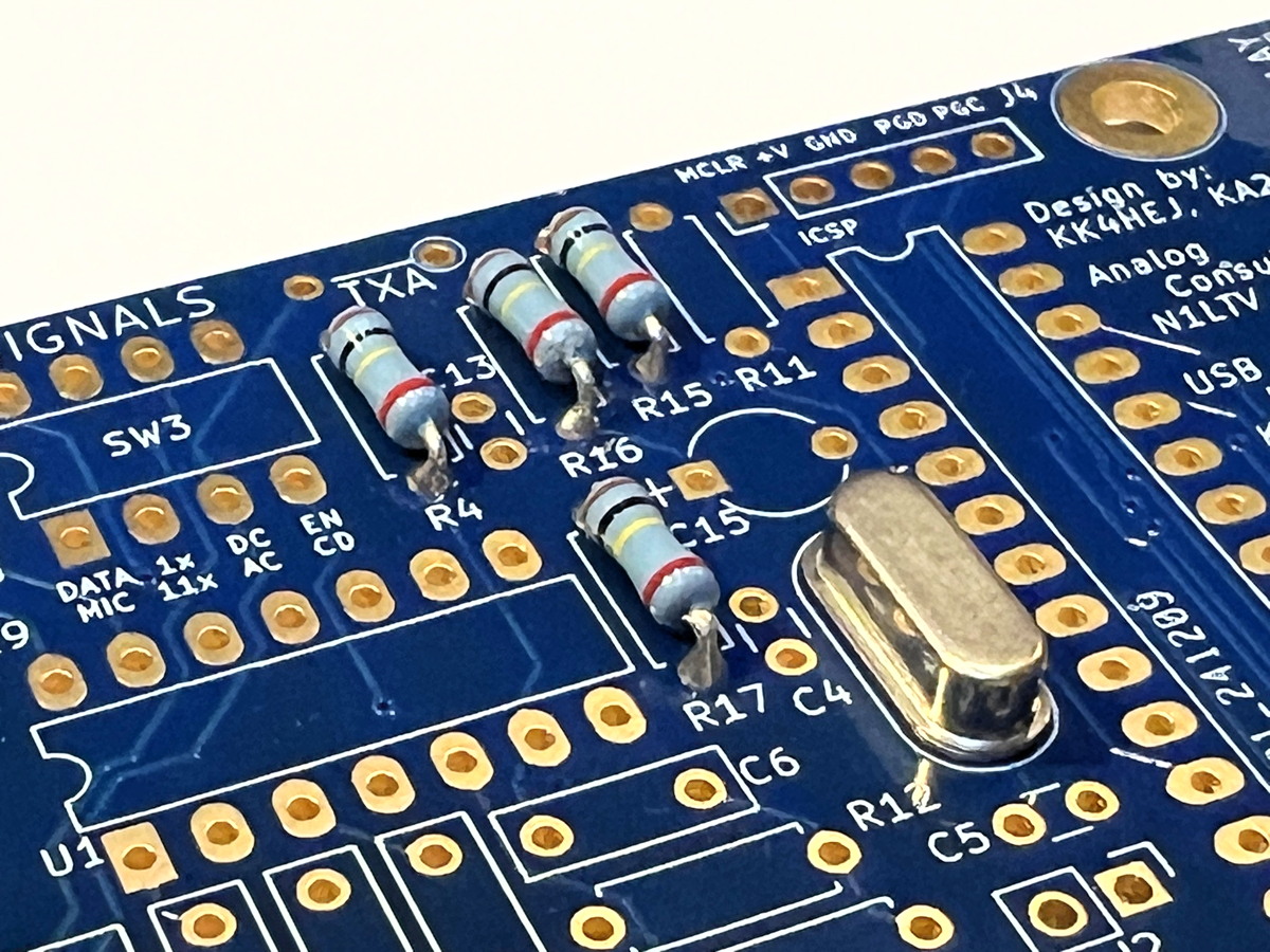
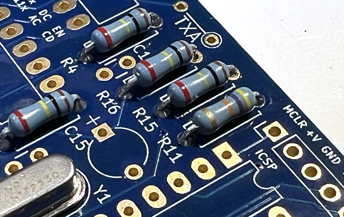
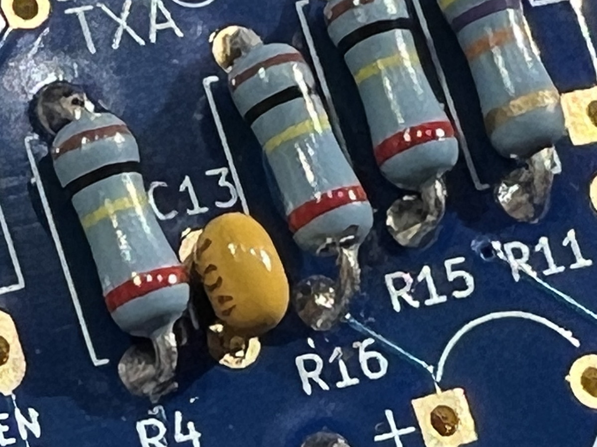
| 2 | R4 R15 R16 R17 |
100 k Ω 5% 1/4 W resistor
brown black yellow 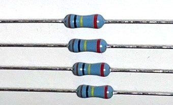
|
R4 is part of the output impedance/level control, along with RV1 - TX Deviation Adjust. R4 is bypassed by the Mic/Data DIP switch.
R4 attenuates the TXA signal to support low-volt, high sensitivity microphone inputs to use NinoTNC
R15, R16 and R17 are a filter in the receive circuit.
 Schematic of RX offset correction and gain stage, highlighting R15, R16 and R17
 (Click to embiggen) 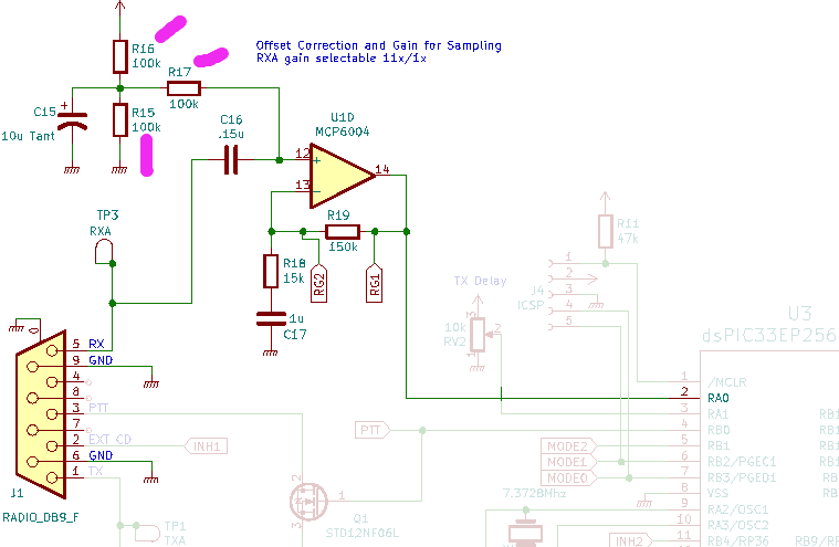
|
| Note: the color codes on the 1% resistors are pretty hard to use. If you are receiving your resistors in a mixed bag of parts, you probably want to do all of the remaining resistor steps before soldering the resistors so you can double check the color codes before you solder and cut. I recommend using a VOM to prove that each 1% resistor is what you think it is, and not one of the other values. |
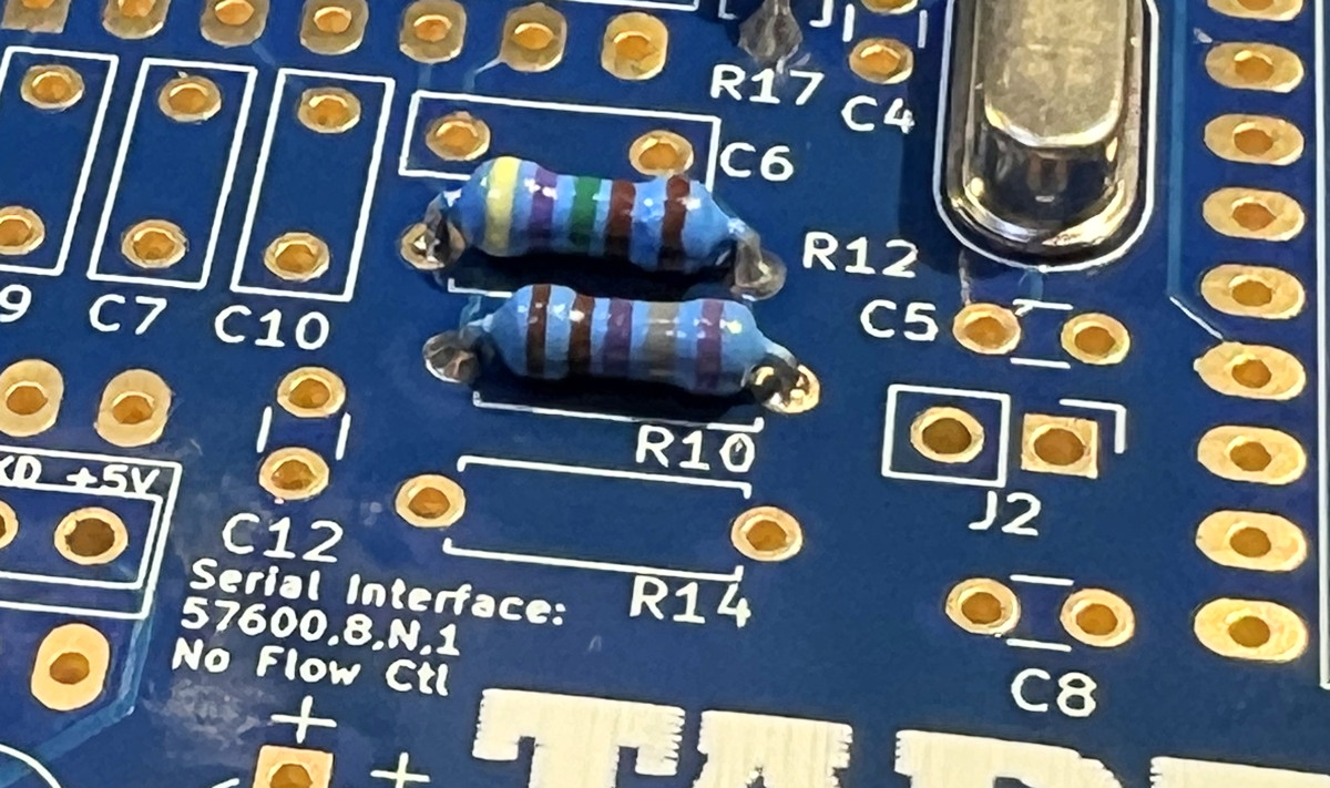
| 3 | R10 | 7.87 kΩ 1% 1/4 W resistor
violet grey violet brown 1% resistors have 3 color bands for value and 1 band for additional 0s. 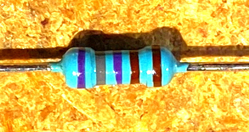
|
This resistor is in the input and feedback loop for the 2nd op-amp stage in the TX-data/audio path.
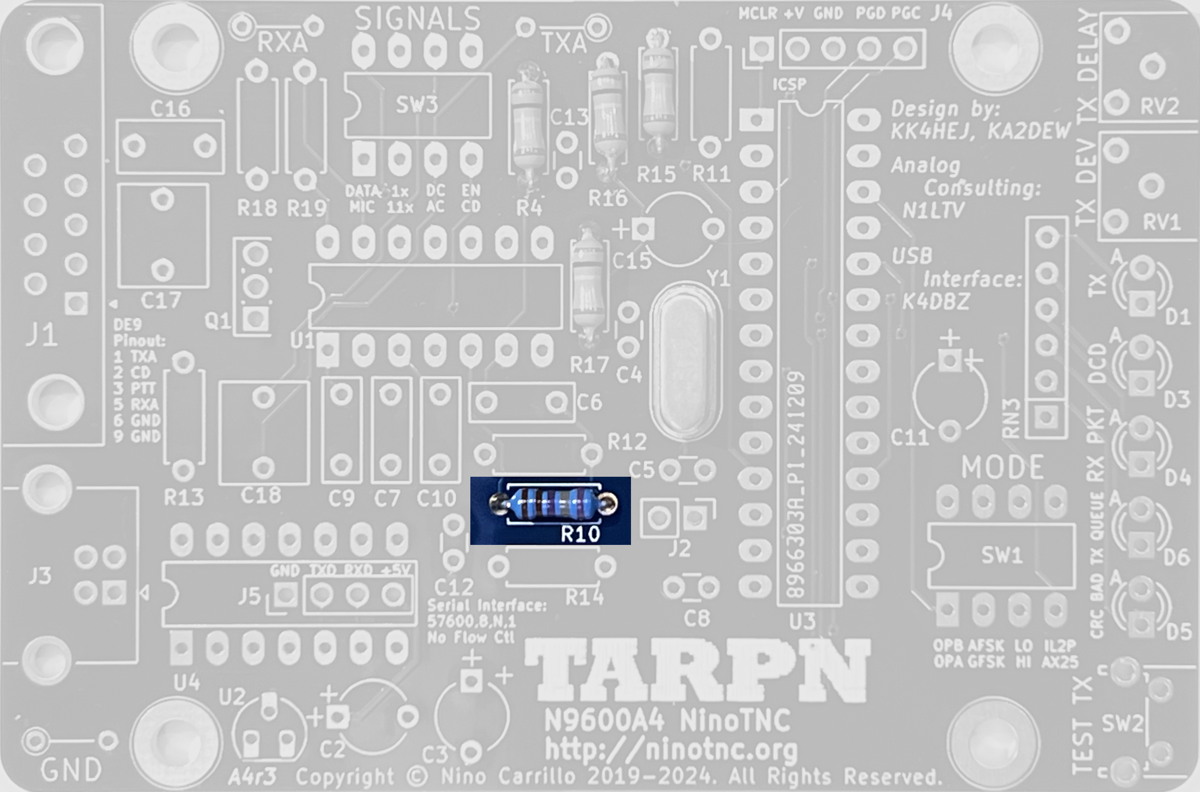
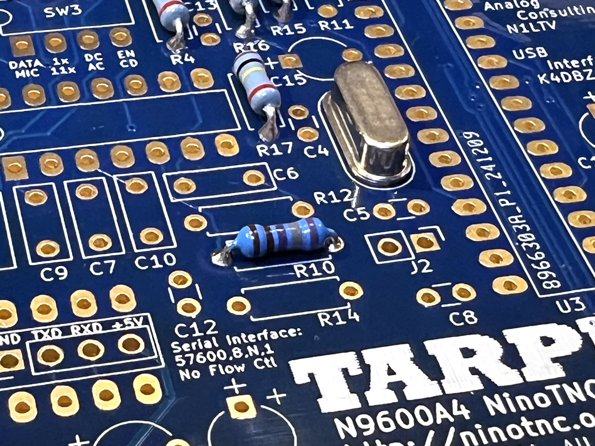 Schematic of TX audio shaping, highlighting R10
 (Click to embiggen) 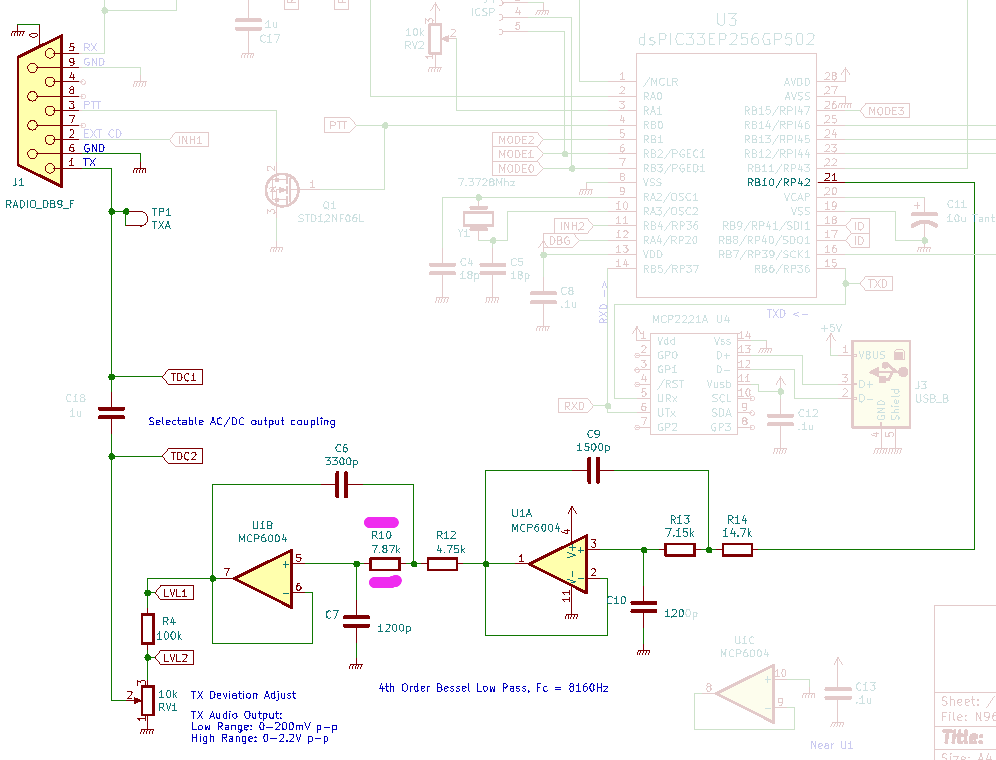
|
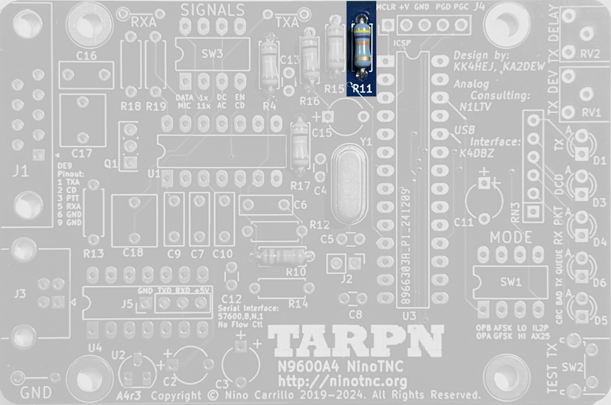
| 4 | R11 | 47 kΩ 5% (or lower %) 1/4 W or 1/8 W resistor
1/8 W shown yellow violet orange 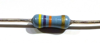
brown or blue body is ok. The stripes are how the part value is read. |
R11 turns off the MCLR input to the CPU in the normal case when a PIC-Kit programmer tool is not attached to the ICSP connector (J4).
The PIC-Kit uses this input to reset the CPU as needed when programming or debugging.
If this resistor is missing, the MCLR line would float across many voltage levels, causing intermittent CPU resets.
 Schematic of MCLR circuit:(Click to embiggen)
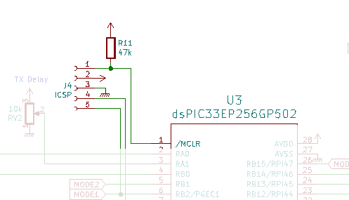
|
| 5 | R12 | 4.75 kΩ 1% 1/4 W resistor
yellow violet green brown 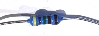 |
This resistor is in the audio path between the 1st and 2nd op-amp stage in the TX-data/audio path.
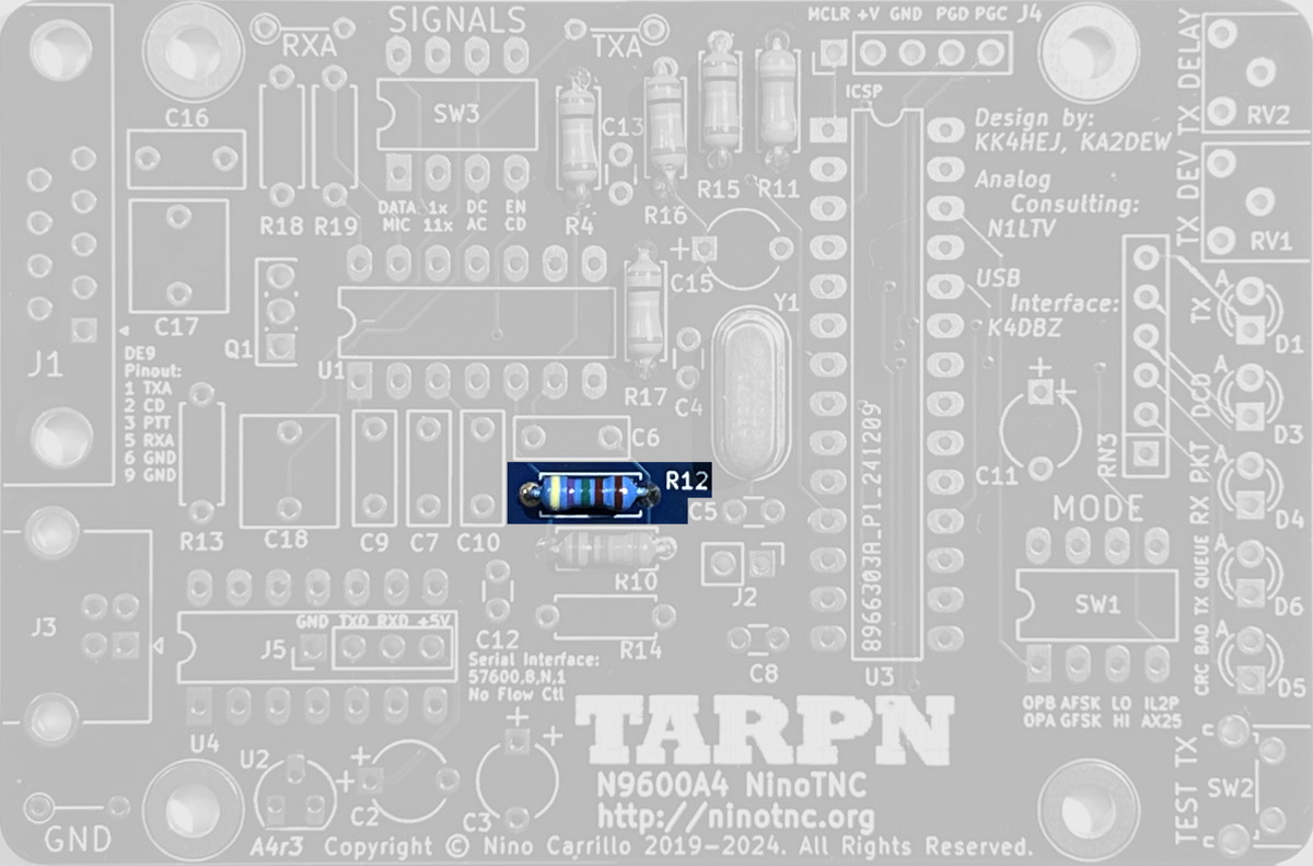
 Schematic of TX audio shaping, highlighting R12
 (Click to embiggen) 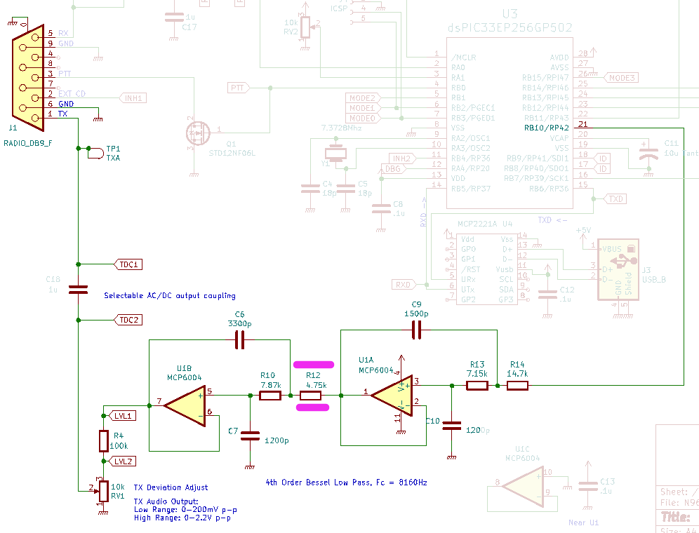
|
| 6 | R13 | 7.15 kΩ 1% 1/4 W resistor
violet brown green brown 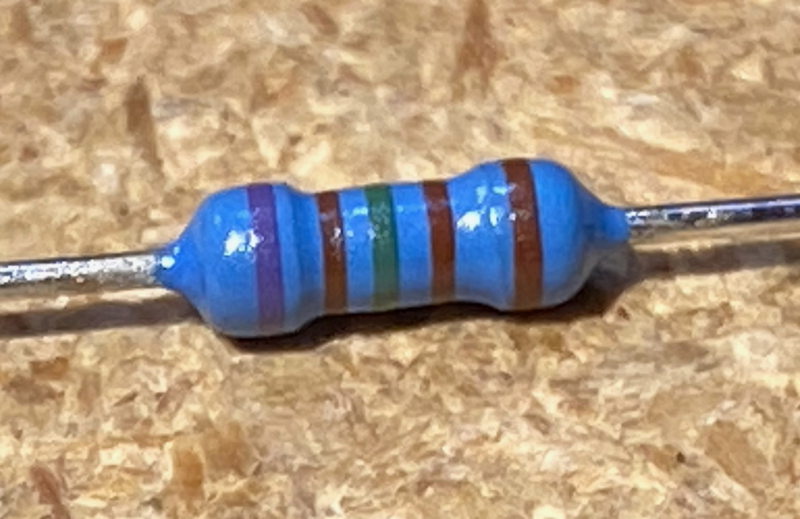 |
This resistor is in the input and feedback loop for the 1st op-amp stage in the TX-data/audio path.
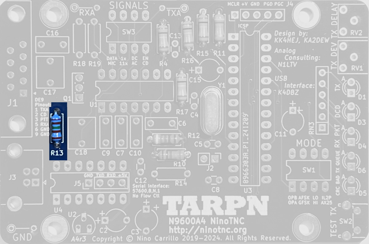
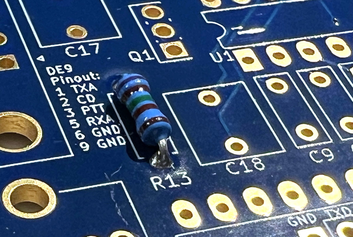 Schematic of TX audio shaping, highlighting R13
 (Click to embiggen) 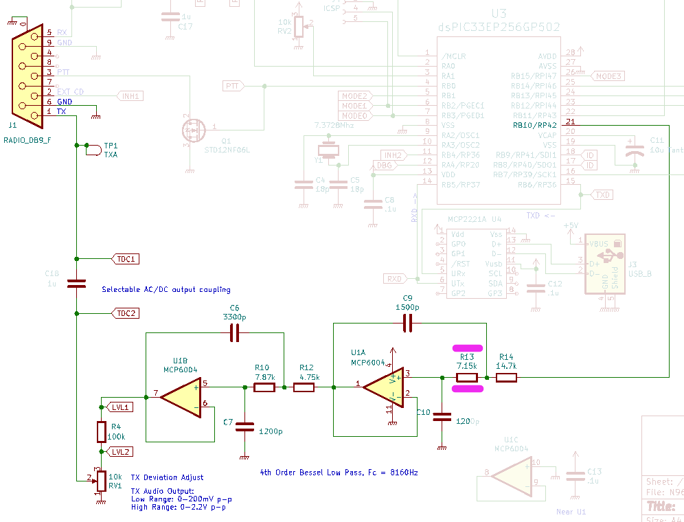
|
| 7 | R14 | 14.7 kΩ 1% 1/4 W resistor
brown yellow violet red 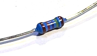
|
This is part of the filter circuit for the 1st op-amp stage in the transmit data circuit.

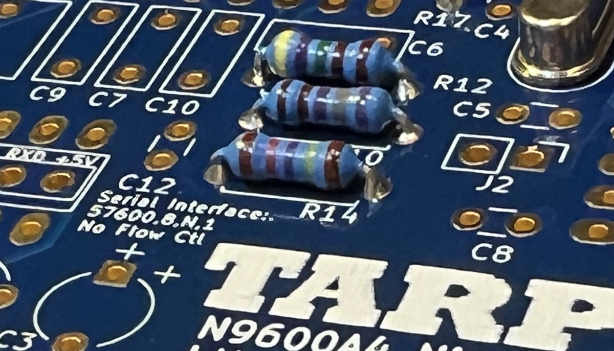 Schematic of TX audio shaping, highlighting R14
 (Click to embiggen) 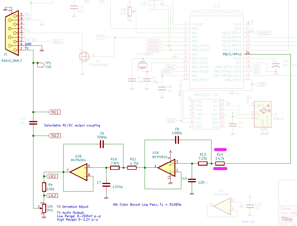
|
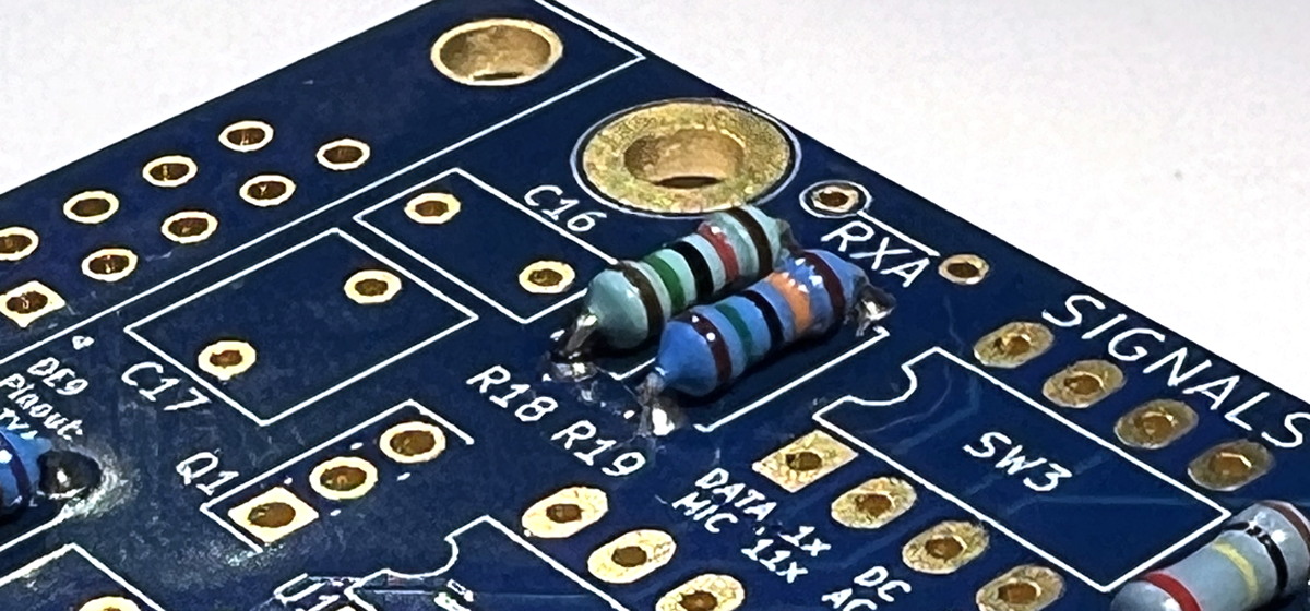
| 8 | R18 | 15 kΩ 5% 1/4 W resistor brown green orange or brown green black red 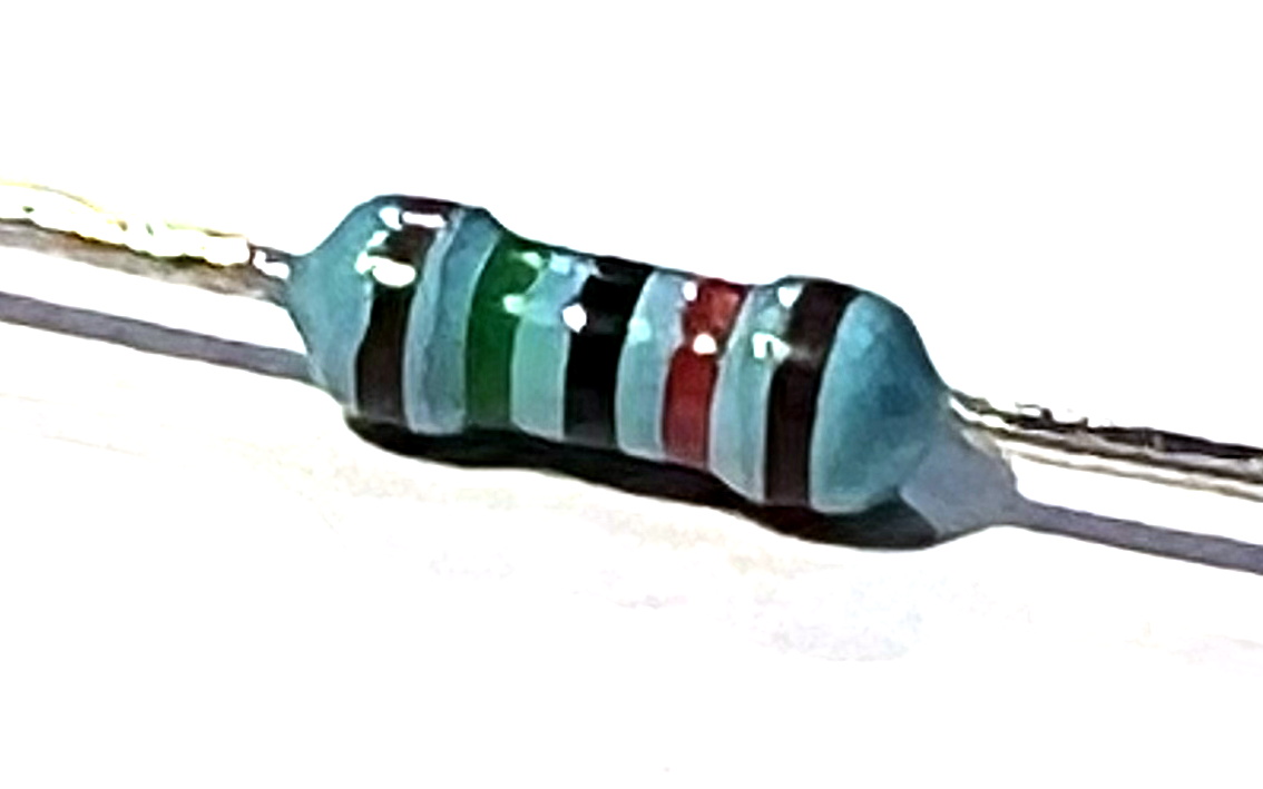
The design calls for a 5% part but based on supply we may choose a 1% part. 1% parts have 4 stripes to describe the value where 5% parts have 3 stripes. 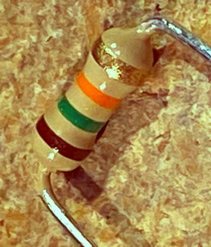
|
R18 is part of the amplification circuit for the Receive audio op-amp.
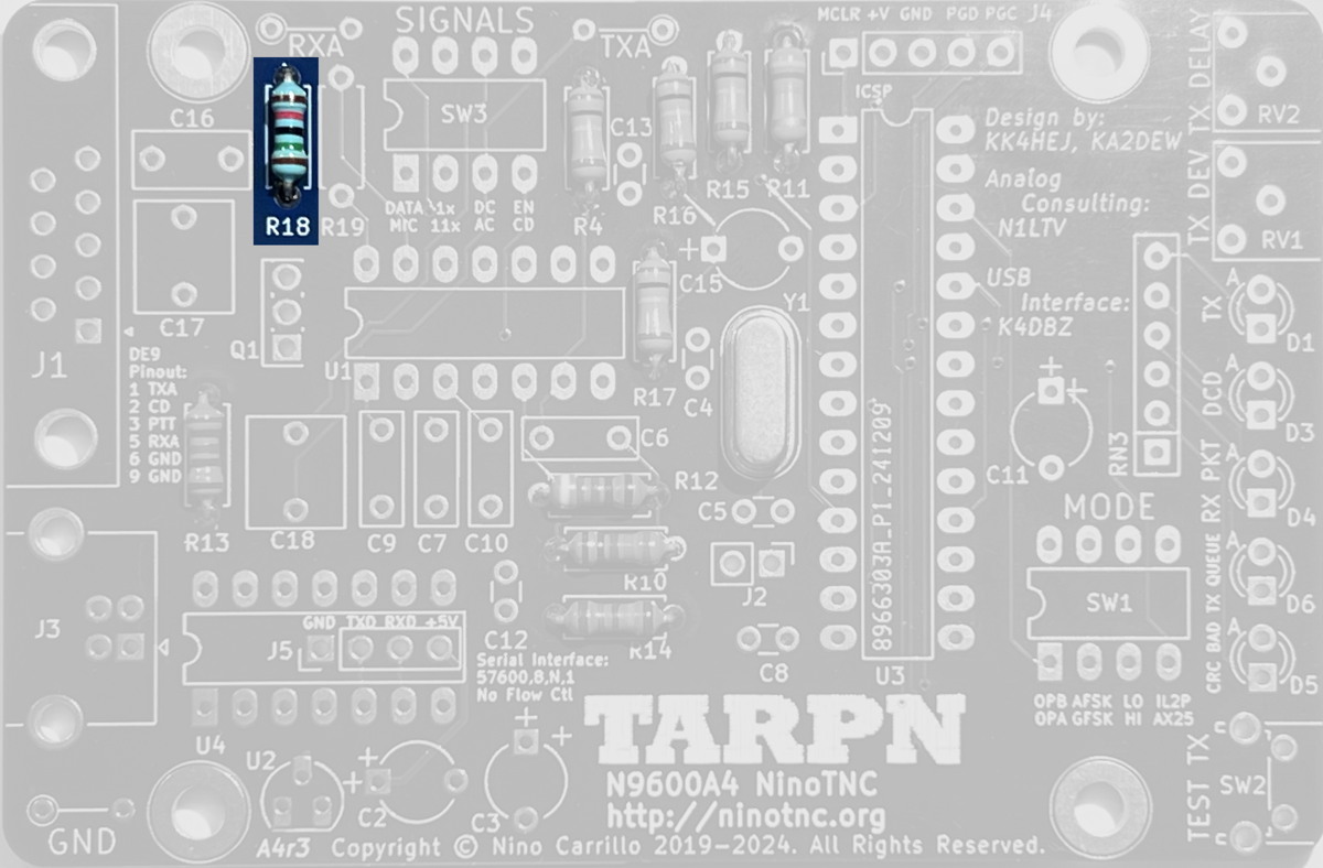
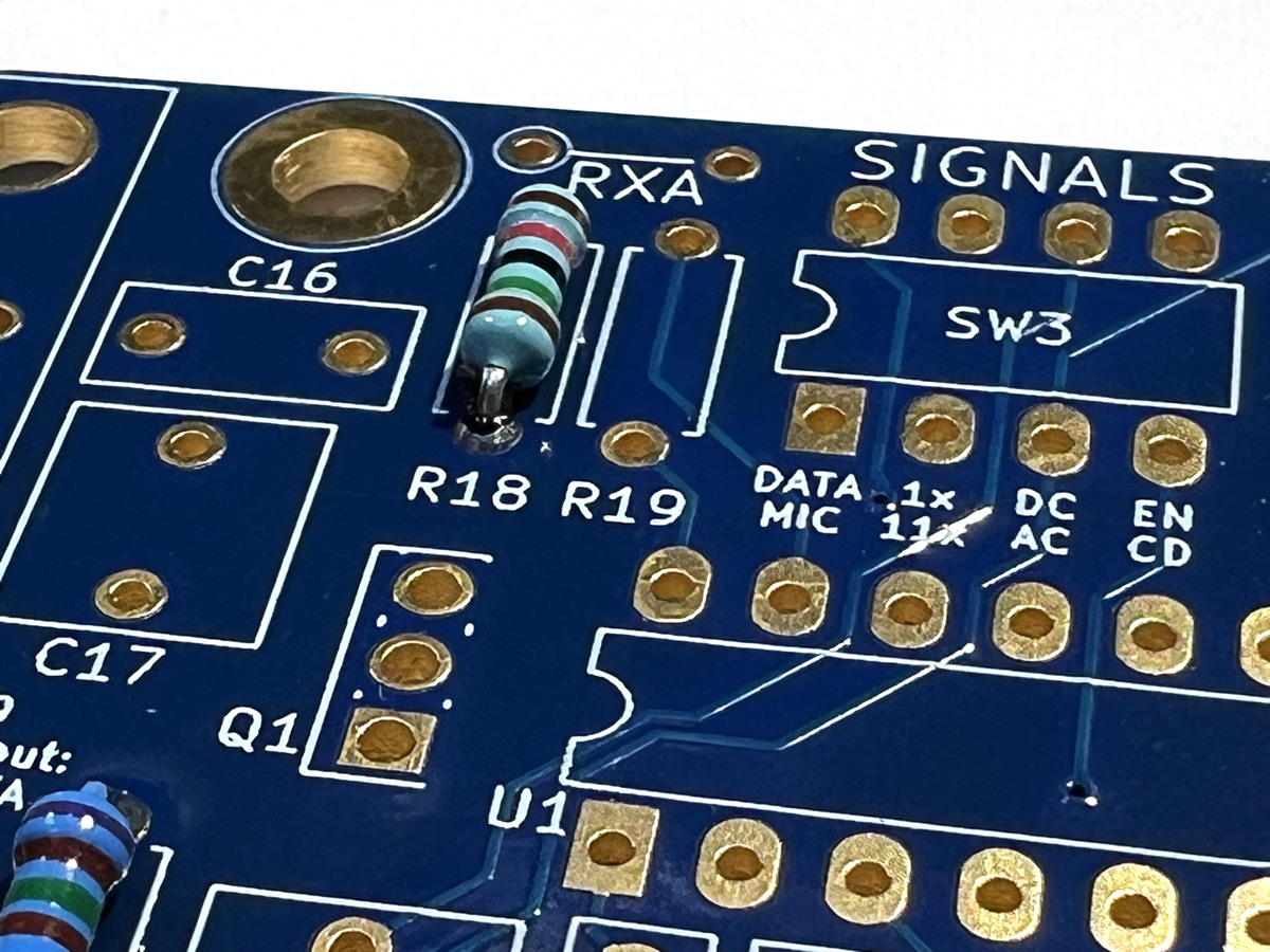 Schematic of RX offset correction and gain stage, highlighting R18
 (Click to embiggen) 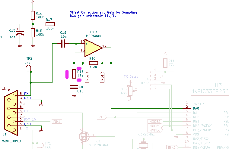
|
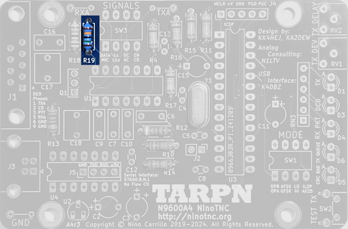
| 9 | R19 | 150 kΩ 5% 1/4 W resistor brown orange black 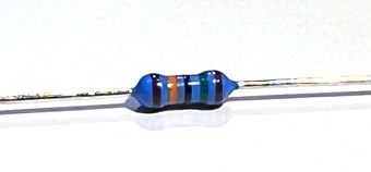 |
R19 is part of the amplification circuit for the Receive audio op-amp.
One of the SIGNALS switches, 1x/11x, bypasses this resistor.
If this resistor is bypassed by the switch in the UP (toward edge of the PCB) position, then the gain of the amp is 11x.
If this resistor is in circuit, switch in the DOWN (toward the TARPN logo) position, then the gain of the amp is 1x, which is also unity gain.
 Schematic of RX offset correction and gain stage, highlighting R19
 (Click to embiggen) 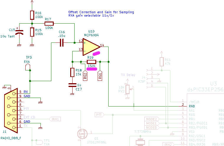
|
| 10 | C4 and C5 | 18 pF 5% 50 V Ceramic capacitor (may be 100 V) marked 18 with a following letter. A substitute part may be blue. 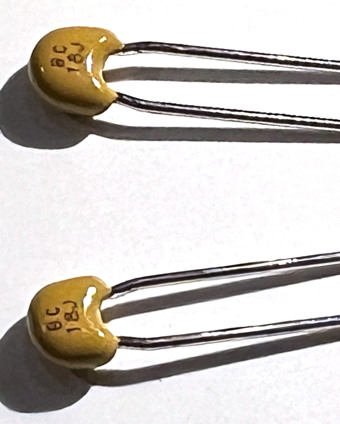 |
C4 and C5 are part of the crystal oscillator circuit
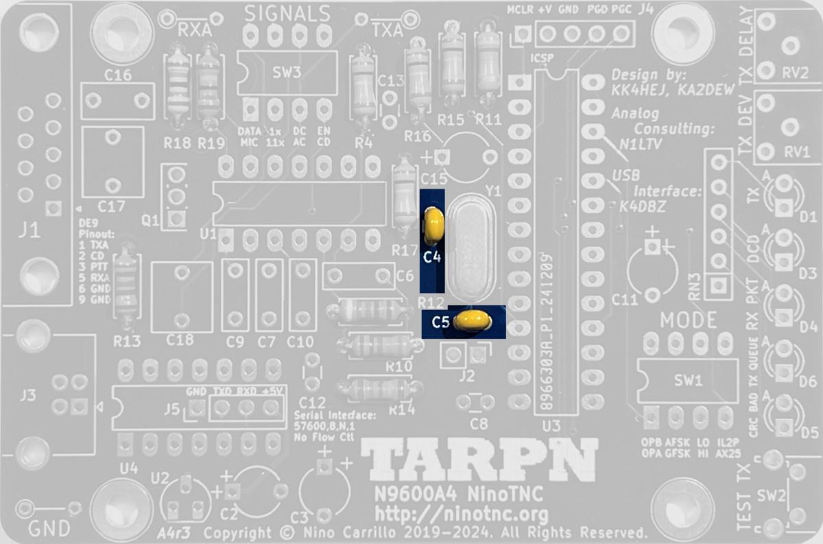
 Schematic showing C4 and C5 in the oscillator circuit:
(click to embiggen)
Schematic showing C4 and C5 in the oscillator circuit:
(click to embiggen)
|
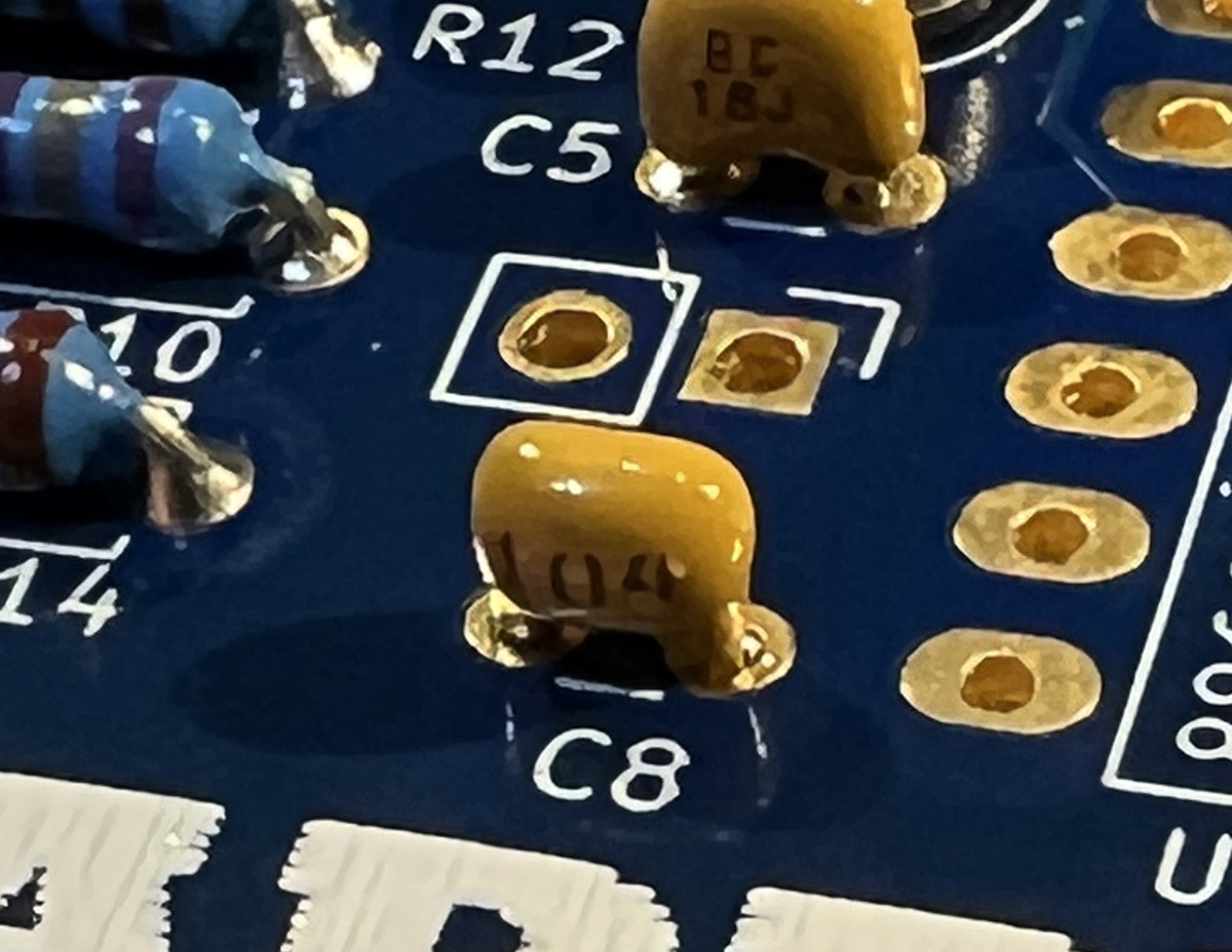
| 11 | C8, C12, C13 | 0.1 µF 10% 50 V Ceramic capacitor
 |
These ceramic radial capacitors provide power supply filtering and glitch reduction on the CPU’s main power input and two other places on the board.
|
| Be careful here. Starting now we'll be installing components which are polarized. That means you have to get each pin in the correct hole. |
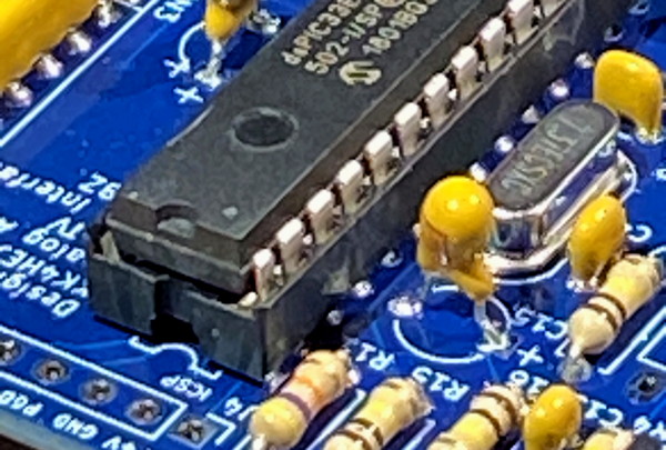
| 12 | XU3 | 28 pin DIP IC socket for U3
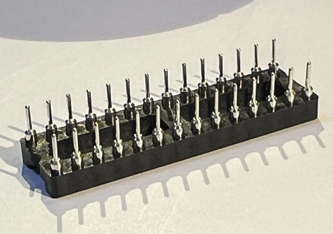
Some 28 pin sockets have flat leads instead of round. | This is the socket for the CPU.
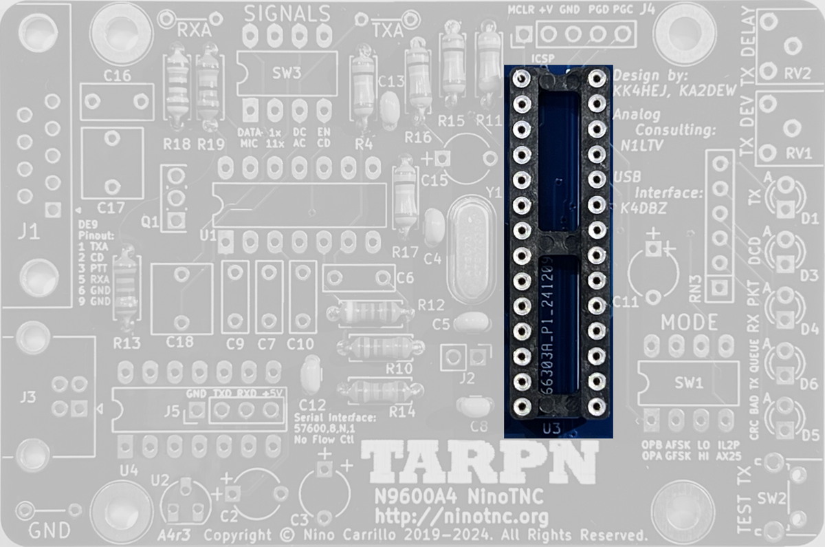
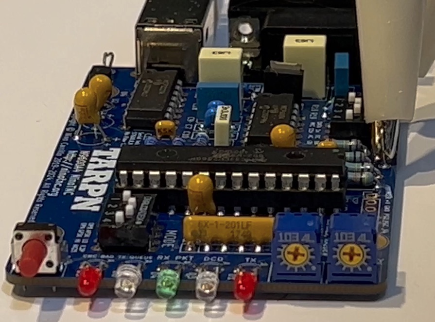
This image has the board upside down - be careful. Here you can see the half-moon is away from the TARPN logo. Click to enlarge.  |
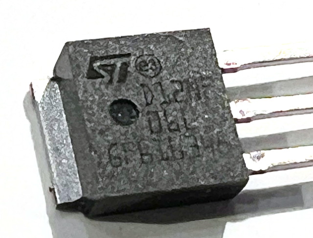
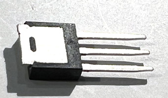
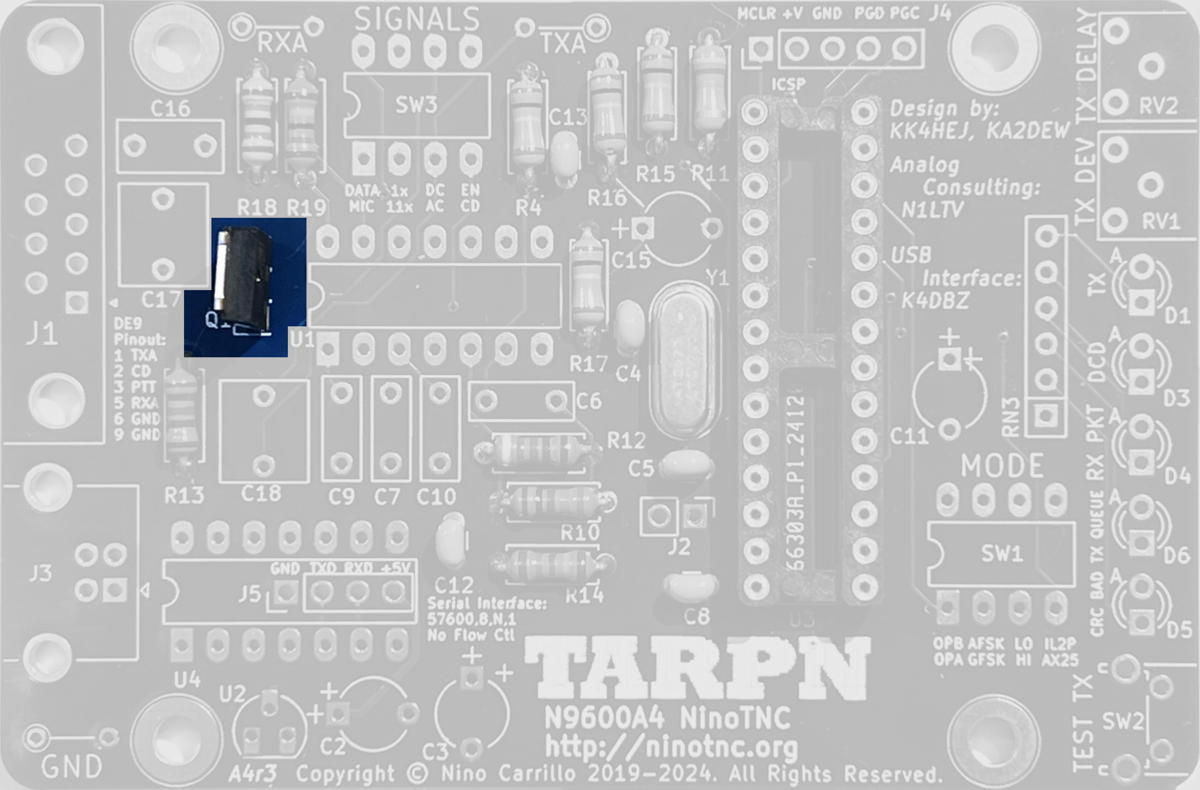
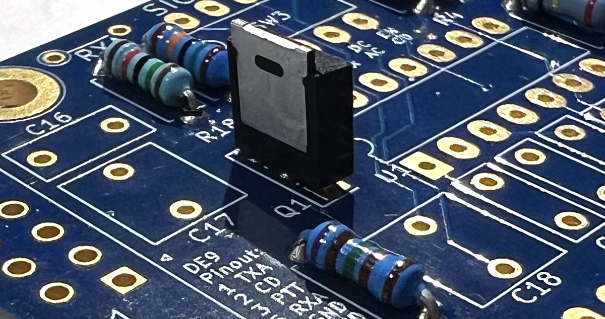
| 13 | Q1 | N-channel MOSFET 100v 1.3amp 3-pin PTT driver.
Metal Oxide Semiconductor Field-Effect Transistor 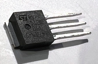
|
A crtical difference in the build instructions between the NinoTNC A4r2 and the A4r3 is the part-footprint of Q1.
In the prior A4 boards, we used a four pin part for Q1.
The manufacturer discontinued all of its 4 pin N-Channel MOSFET devices.
We have changed manufacturers and now we use a STMicro 3-pin N-Channel MOSFET part# STD12NF06L-1.
Install so the metal side of the part is facing toward C17 and J1.
See the photos.
|
|
Circuit Description:
When used with a microphone, the measured voltage on the PTT wire is whatever the radio generates. When the microphone button is squeezed, the PTT wire is grounded to the radio ground, bringing the voltage to a relative 0 V. The radio's circuit will see the 0 V and will go into transmit. When the PTT wire is released by the microphone's switch, the radio's power will drag the wire back above 0 V/Ground and now the radio's circuit will go into receive mode. This MOSFET device is driven by a GPIO (single wire control output) on the NinoTNC dsPIC CPU. The MOSFET is responsible for pulling the PTT line to ground when the NinoTNC wants to send a packet. The MOSFET takes a turn-on signal, in the form of very little current at 3.3v, from the dsPIC CPU. If no turn-on current is present, the output of the MOSFET is allowed to float. The radio will provide a pull-up voltage back along the PTT wire and that wire will be seen to be not at ground 0V level. When used with NinoTNC A4, the PTT wire is fed into, or out of, the TNC through the DE9 connector, directly to the MOSFET pin 2. If the NinoTNC CPU is not asserting its turn-on signal to pin 1 of the MOSFET, pin 2 is dragged up by the radio's PTT voltage. When the NinoTNC CPU asserts 3.3 volts onto its GPIO output, wired directly to pin 1 of the MOSFET, the MOSFET shorts pin 2 through its internal diode to pin 3, which is grounded to the NinoTNC and to pin 9 of the DE9 connector. When the NinoTNC CPU is asserting the PTT as active, the 3.3v also drives LED D1 to turn on. Note that the LED can function even if the MOSFET is completely missing, so D1 illuminating is not a sign that the MOSFET is installed correctly or working. The other design consideration is that we want to prevent leakage between the PTT wire from the radio into the CPU. With the TNC we started with, the TNC-PI, it looked like it was possible for the CPU to power itself from the leakage through the NPN transistor. We went with the N-channel MOSFET, instead of the NPN transistor, just to be sure. 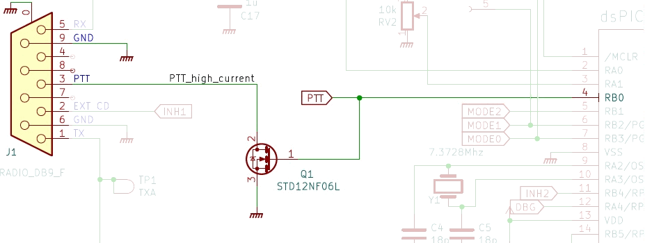
|
|||
| 14 | U2 | MCP1702 3.3 V or
MCP1700 3.1 V 250 mA TO92 case regulator 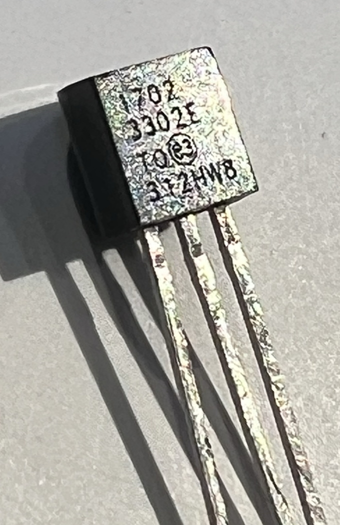 |
This part takes the 5 V DC from the USB connector and regulates it down to 3.3 V or 3.1 V, to fall within the 3.0 to 3.6 V operating range of the dsPIC CPU.
Align flat edge with the board silkscreen 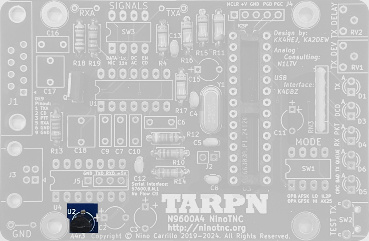
 Here is the schematic showing the regulator and its two caps.
I talk about this circuit fragment again in the step where you add the two capacitors.
Here is the schematic showing the regulator and its two caps.
I talk about this circuit fragment again in the step where you add the two capacitors.
 |
| 15 | RN3 | 5 resistor 180 Ω resistor network
Substitute may be a 220 Ω resistor network 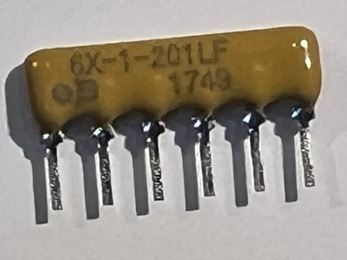
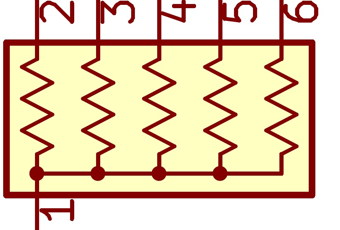
|
Orientation is important!
Pin 1 is identified by the square around the hole on the PCB and an interesting symbol near the end pin on the component. See schematic symbol below. I had good luck by folding two of the leads in opposite directions to hold the part in place before soldering. Once you fold the two pins, align the part upright, then solder. This five-resistor network provides an in circuit resistance to limit the LED current for each of the 5 LEDs 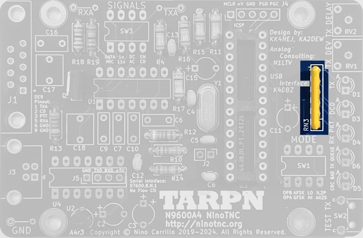

|
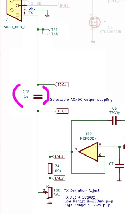
| 16 | C17, C18 | 1 µF [metal] film capacitor radial leads 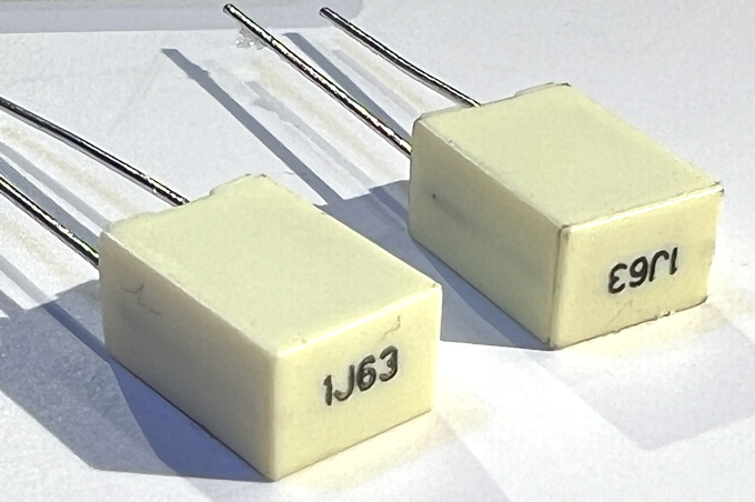 |
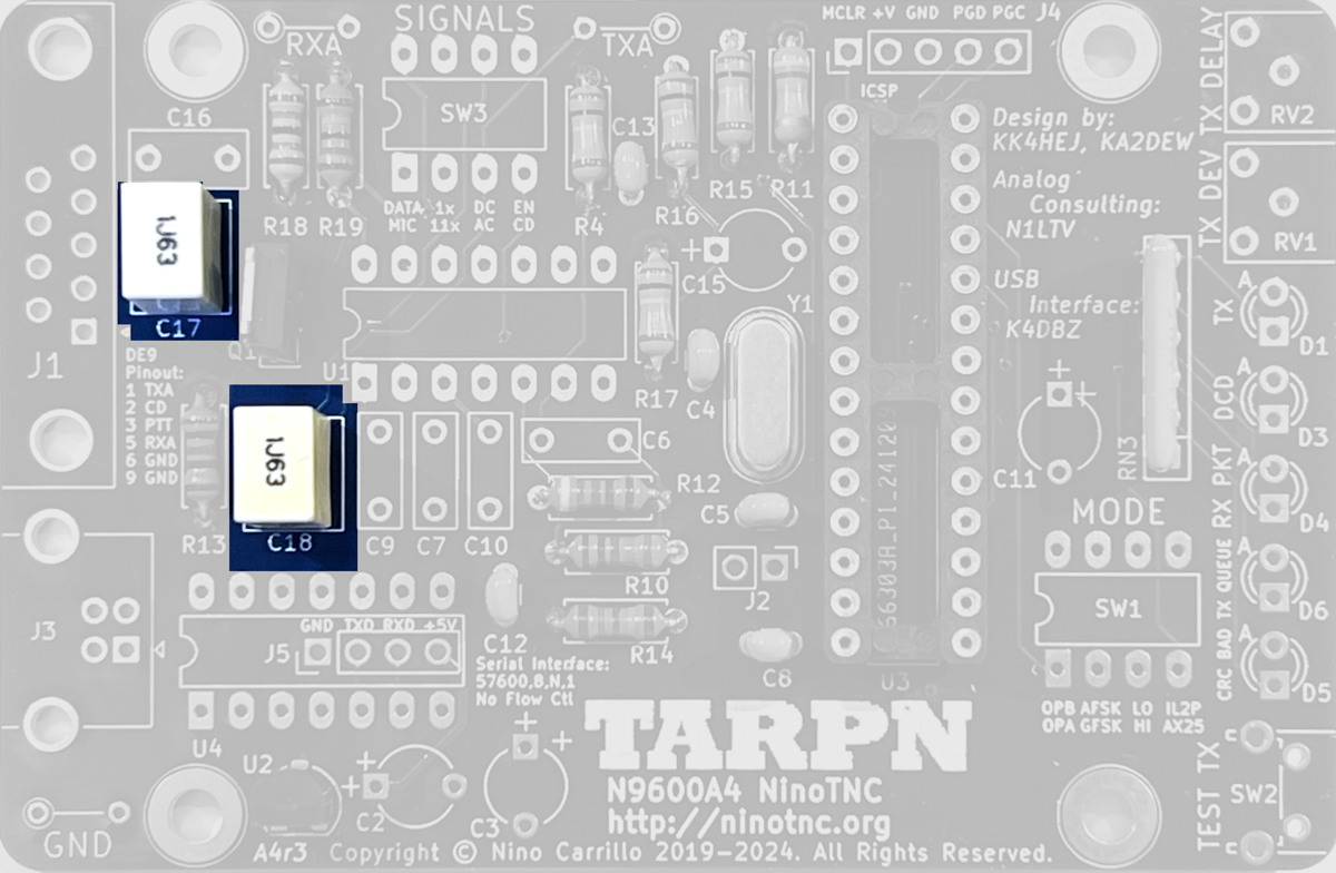
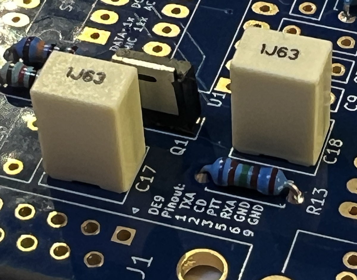 Capacitor C17 is part of a receiver filter between the DE9 and the CPU.
 Capacitor C18 provides AC-coupling just before the DE9 [radio] connector on the TXA circuit.
SIGNAL switch SW3 may select DC-coupling which bypasses (shorts) C18.
AC-coupling has the effect of moving AC (audio) waveforms to be relative to the radio's neutral level.
The input to C18, in NinoTNC's TXA output circuit, is alternating current audio wich is relative to the final op-amp's output.
In the NinoTNC's case the transmit audio output from the op-amp chip is elevated by 1.65 volts, so the negative going side of a sine wave could be just barely above 0 volts, where the positive going side is nearly at 3.3v.
This 1.65 volts is called a DC offset.
If DC/AC switch is off, i.e. AC, the TXA output goes through C18 and the DC offset is removed from the signal.
Having the DC/AC switch set to off (i.e. AC-coupled) is the prefered mode of operation of the NinoTNC, at least at this time.
Capacitor C18 provides AC-coupling just before the DE9 [radio] connector on the TXA circuit.
SIGNAL switch SW3 may select DC-coupling which bypasses (shorts) C18.
AC-coupling has the effect of moving AC (audio) waveforms to be relative to the radio's neutral level.
The input to C18, in NinoTNC's TXA output circuit, is alternating current audio wich is relative to the final op-amp's output.
In the NinoTNC's case the transmit audio output from the op-amp chip is elevated by 1.65 volts, so the negative going side of a sine wave could be just barely above 0 volts, where the positive going side is nearly at 3.3v.
This 1.65 volts is called a DC offset.
If DC/AC switch is off, i.e. AC, the TXA output goes through C18 and the DC offset is removed from the signal.
Having the DC/AC switch set to off (i.e. AC-coupled) is the prefered mode of operation of the NinoTNC, at least at this time.
 |
| 17 | C2, C3, C11, C15 | 10 µF 10% 16 V tantalum dipped capacitor 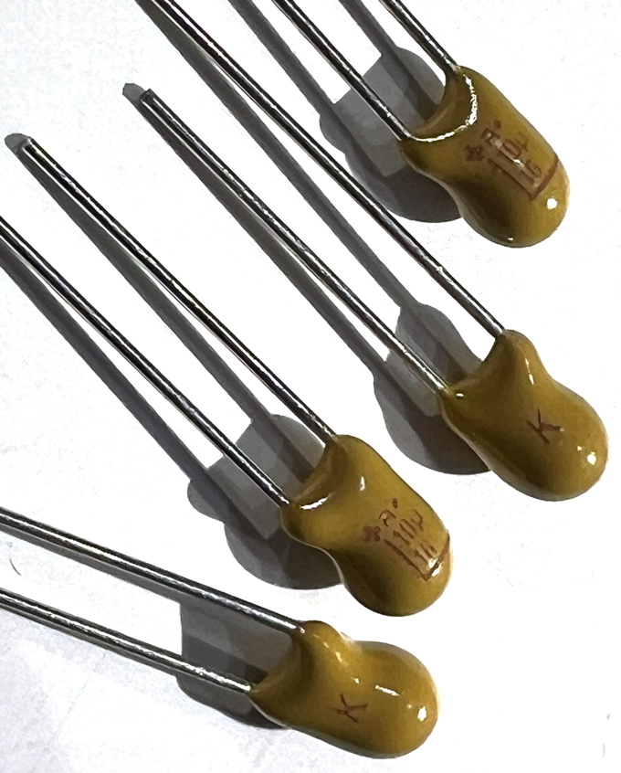
|
Carefully observe values and polarities.
Positive side is marked with a very small plus sign on the part, or a red stripe, and the pin nearest the + goes into the square solder pad/hole on the PCB.
The silk-screen also has a + sign, to remind you.
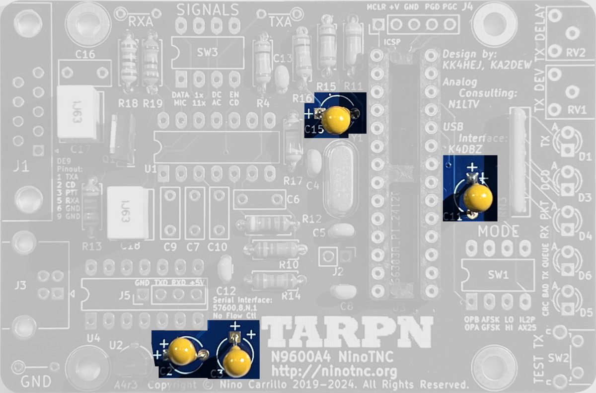
C2 is 5v filter on the input to the regulator. C3 is the 3.3v filter on the output from the regulator.
C11 is vcap input to the CPU on one side and ground on the other. VCAP is a pin on the Microchip CPU used for an internal filter. I'm guessing this is to make the Analog to Digital converter input more stable. C15 is part of a receive filter circuit, along with C1 R15 R15 R17, between the DE9 and the first receive op-amp stage. 
C2 and C3 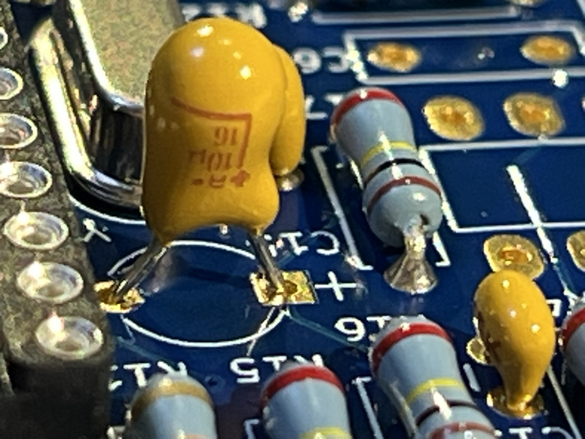
C15 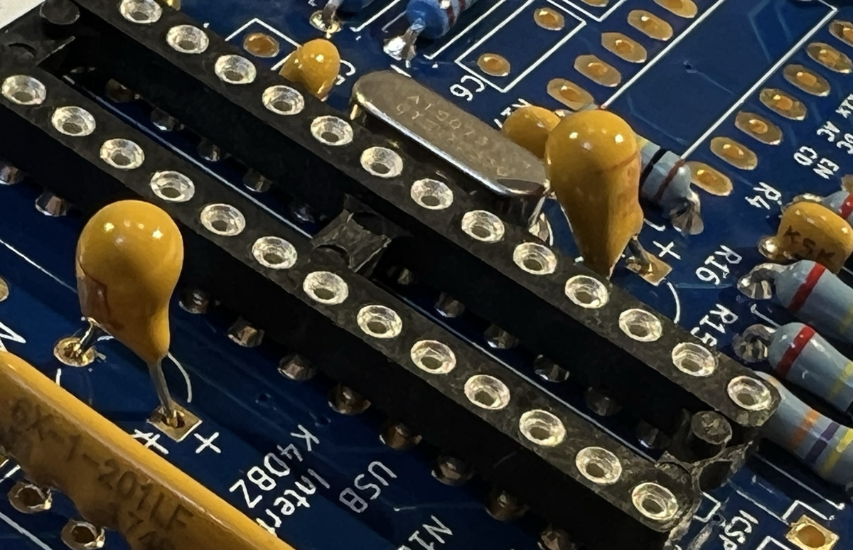
C11 and C15 |
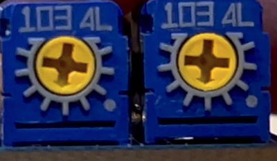
| 18 | RV1 and RV2 | 10 kΩ 1/2 W cermet 1-turn side adjusted trimmer potentiometers.
Label="103" 10 * 10**3 = 10000 Ω. 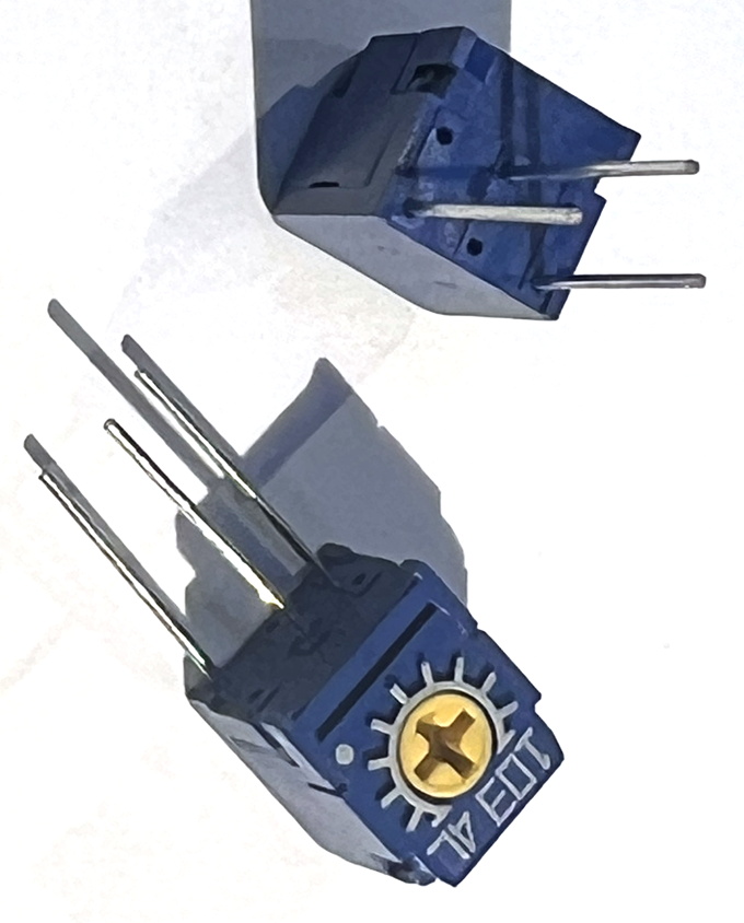
On the face of the part, notice the arrow on one of the legs of the yellow cross. It is pointing down in this image. This will be important when operating the NinoTNC. If necessary, RV2 (TXDELAY) can be a larger value, up to 100 kΩ. The part may have been replaced with a 2nd source of a part which is a different color and a little more open-frame looking. 
|
Note: In March 2025 the blue parts shown in the photos, which are NIDEC CT-6EX103, became out of stock at Mouser.
We substituted a TT 36WR10KLF which looks totally different but is electrically and physically compatible.
Personally, I think the NIDEC part looks better. If you agree and are willing to pay an extra shipping charge, Digikey has the NIDEC in stock. According to Mouser, they'll have the NIDEC unit back in stock in May 2025. Place the two parts side by side in the appropriate holes. The screwdriver adjustable end faces the edge of the board. Solder one pin on each part. Hold each part with a finger while heating the one pin so the solder melts and the part can be pressed flat to the board. Let the solder harden, and then solder the other two pins. Finally, go back and wet the original pin and let the solder reflow around the pin. 
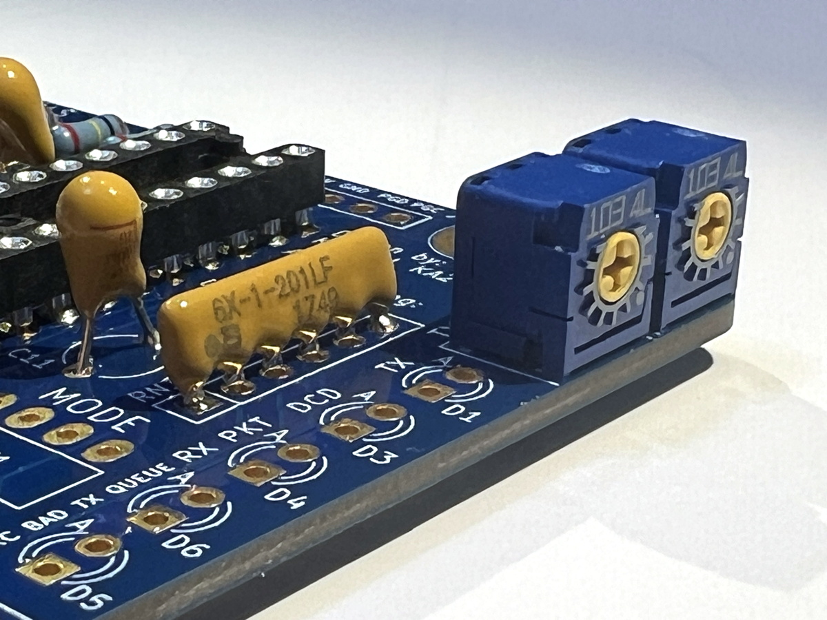 TXLEV RV1 adjusts the Tx Audio level at the output of the TXA op-amp pair.
Schematic highlighting RV1 (Click to embiggen) 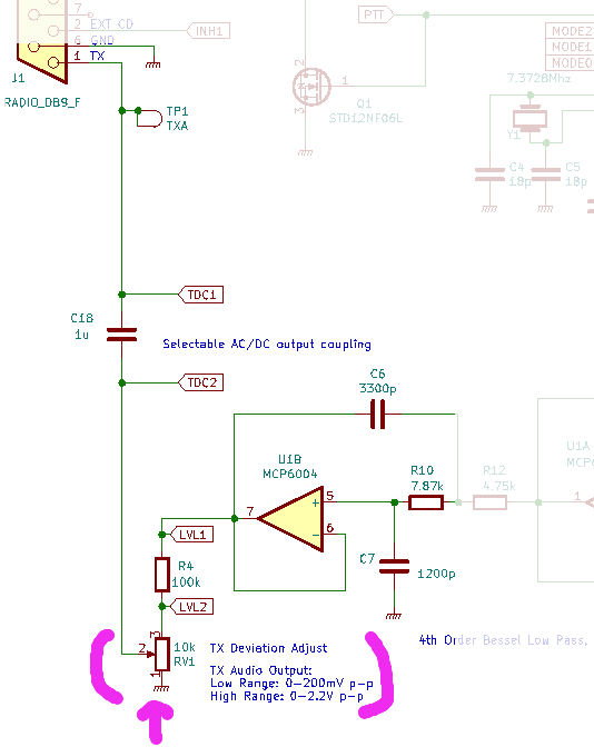 TXDELAY RV2 adjusts an input to the CPU and is used by the program to set the transmit preample duration.
This preamble compensates for the time needed for the transceiver to switch from receive to transmit.
TXDELAY RV2 adjusts an input to the CPU and is used by the program to set the transmit preample duration.
This preamble compensates for the time needed for the transceiver to switch from receive to transmit.
Schematic highlighting RV2 (Click to embiggen) 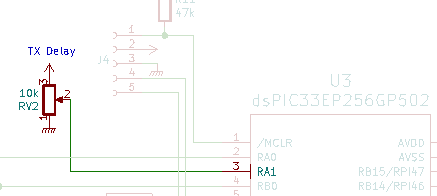
|
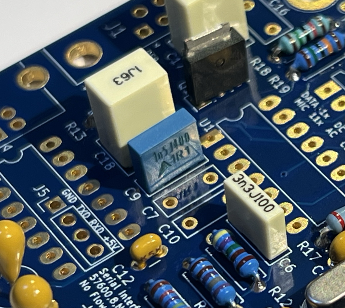
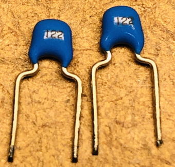
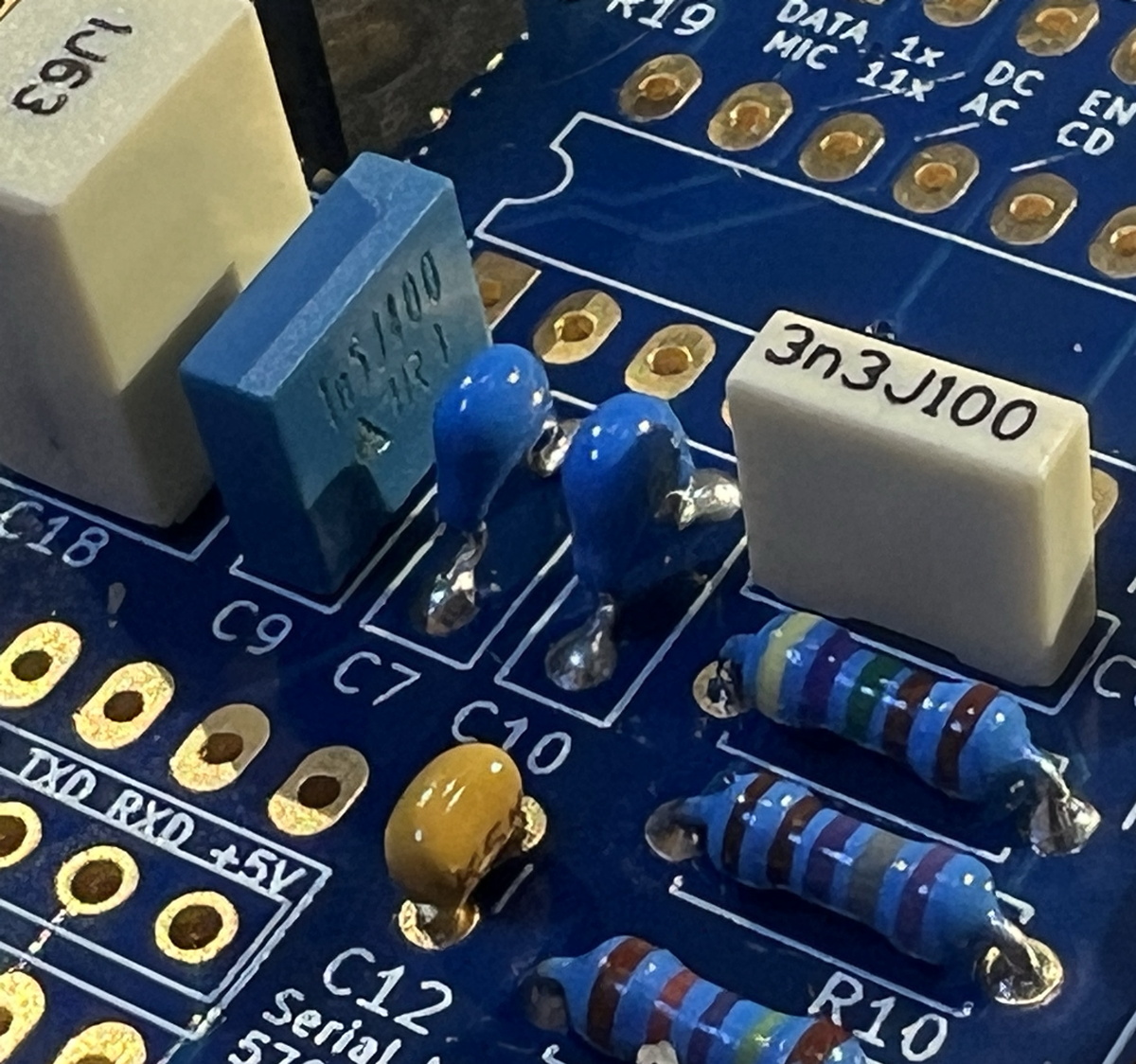
| 19 | C6 | 3300 pF [metal] film capacitor radial leads 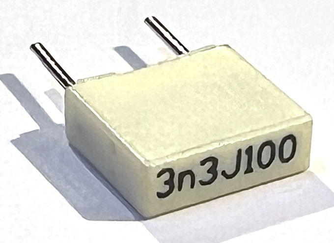
This part may be blue or yellow. This part also may be the same color as C9. Read the bag label and part label carefully. |
This is part of the feedback loop in the 2nd stage of the transmit data output.
A wrong value here could hurt the readability of your packets.

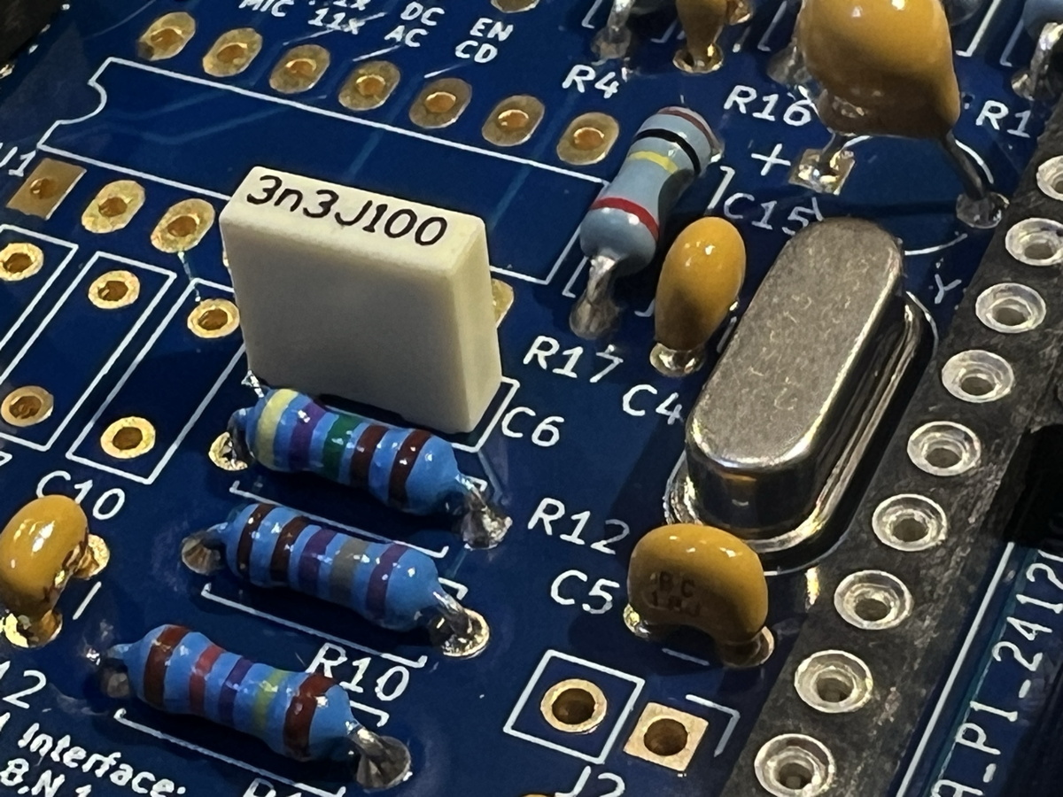 Schematic of TX audio shaping, highlighting C6:
 (Click to embiggen) 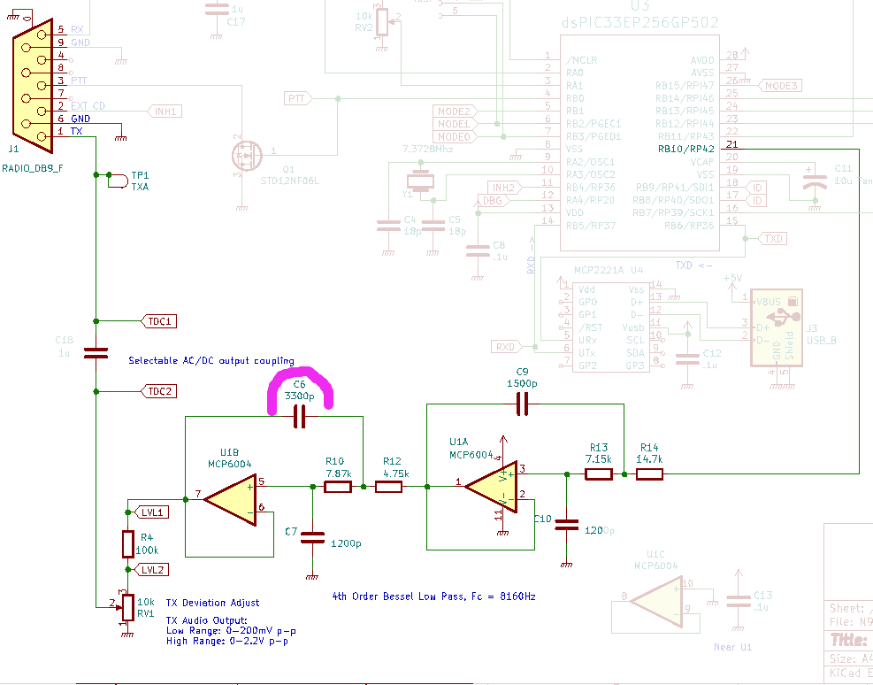
|
| 20 | C9 | 1500 pF [metal] film capacitor radial leads 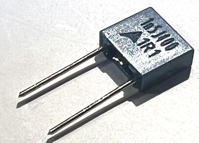
This part may be blue or yellow. This capacitor may look just like C16. Look at the bag label and/or the part label carefully! |
This is part of the feedback loop in the 1st stage of the transmit data output.
A wrong value here would make your packets hard to decode while the loopback test might pass!
 Schematic of TX audio shaping, highlighting C9:
 (Click to embiggen) 
|
| 21 | C16 | CAP FILM 0.15UF 5% 100VDC 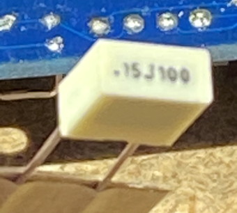
White or blue package. This capacitor looks just like C9. Look at the label carefully! 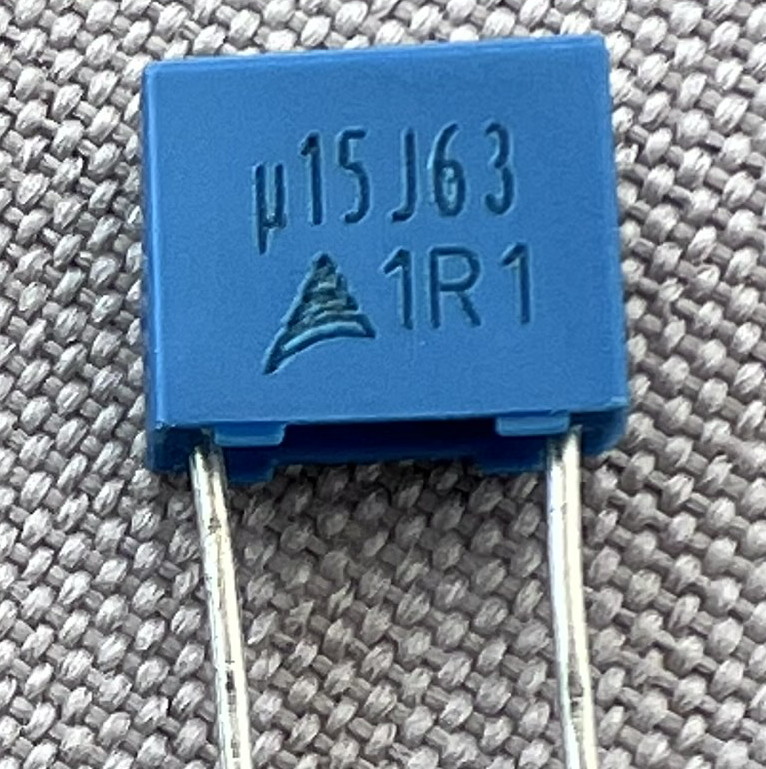 |
This capacitor is in the receive audio and serves to remove a DC voltage offset from the received audio. If this part is missing, there won't be any receive audio. See schematic below. 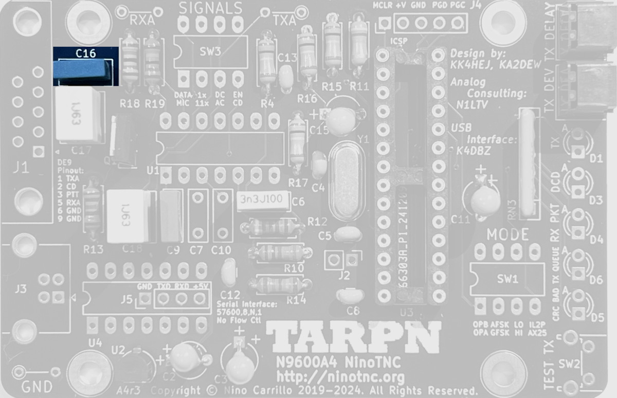
 Schematic of RX offset correction and gain stage, highlighting C16:
 (Click to embiggen) 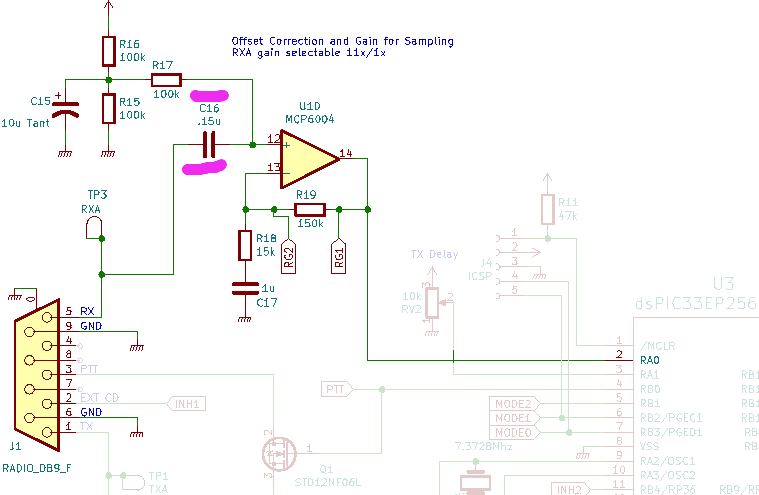
|
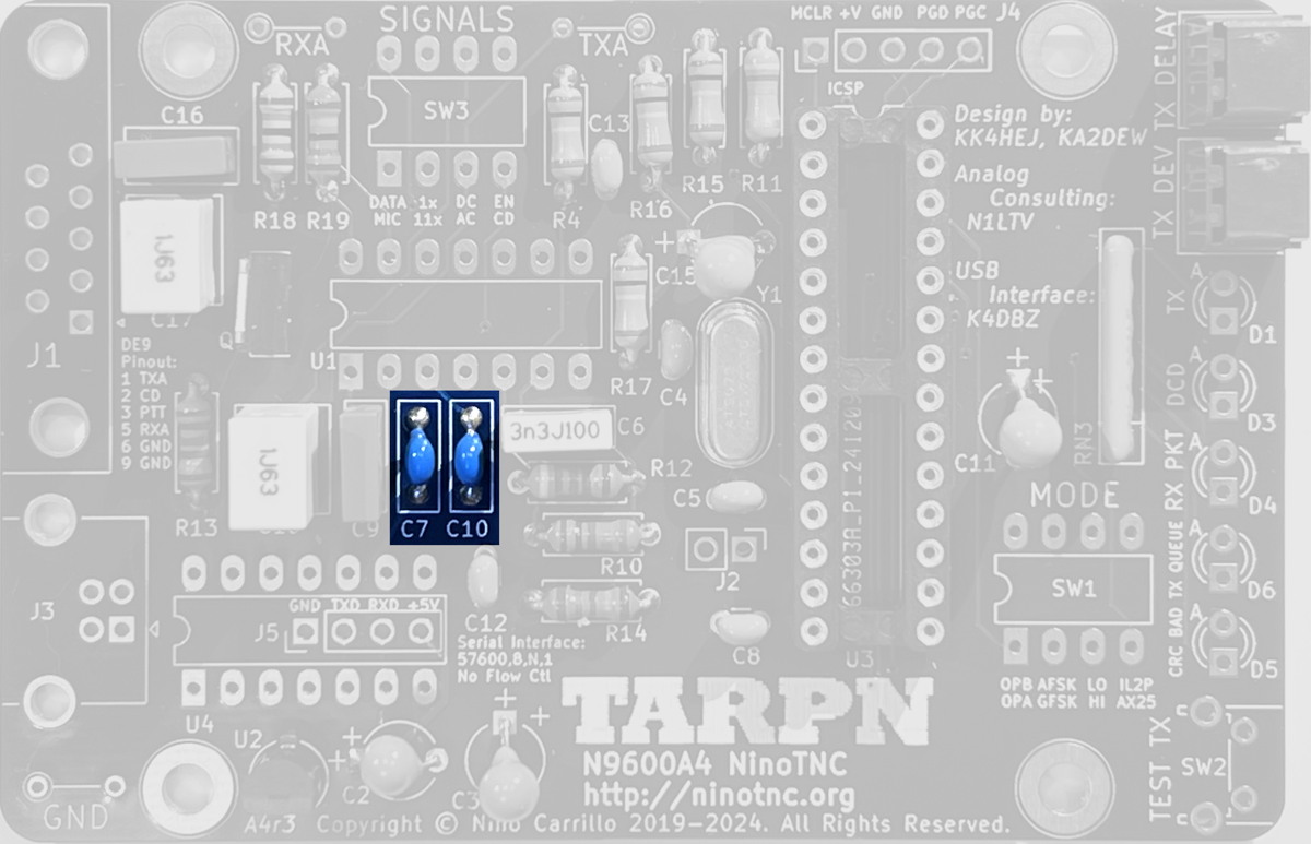
| 22 | C7, C10 | 1200 pF 50v capacitor
light-yellow polyester-film or blue ceramic 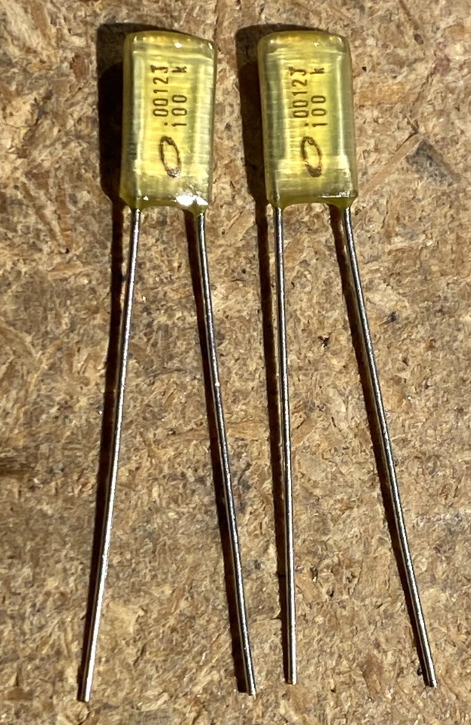
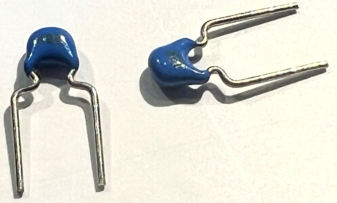
|
In the transmit Op Amp chain, these two capacitors are across the input on each of the first two stages.
These capacitors serve as part of a filter to reduce the high frequency audio noise that will be transmitted.
 Schematic of TX audio shaping, highlighting C7 and C10
(Click to embiggen) 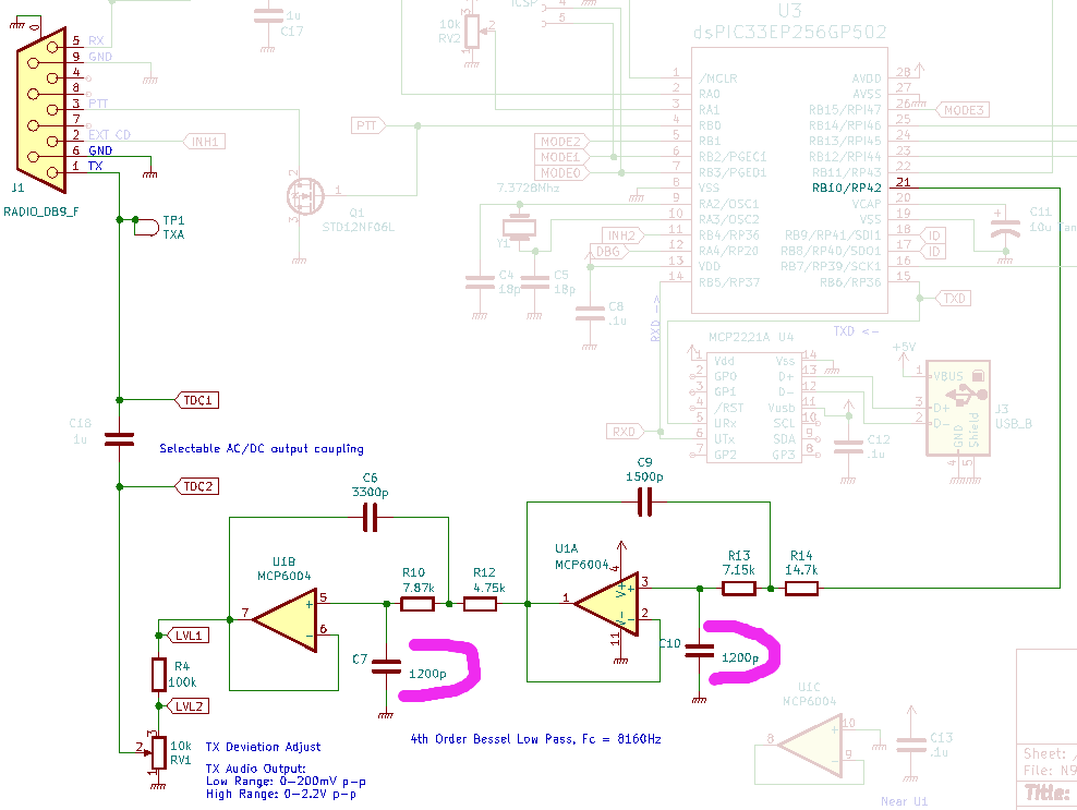
|
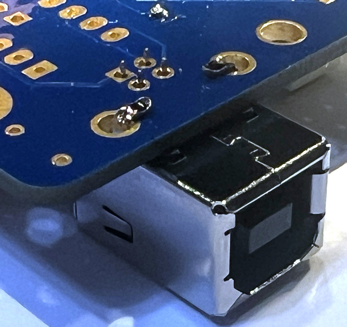
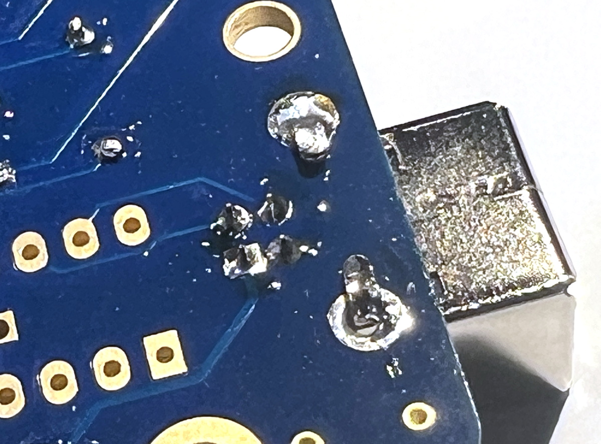
| 23 | J3 | USB-B socket
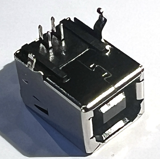
|
This socket has six solder points, two of which look like they'll get in the way when you insert them.
They don't.
But they will hold this connector onto the PCB.
After inserting the connector onto the board, inspect the four data pins. Bend the two heavy tabs toward each other, securing the connector. Solder one of the pins, then wet it again while forcing the connector onto the board. Then solder the other three pins followed by the two support tabs. 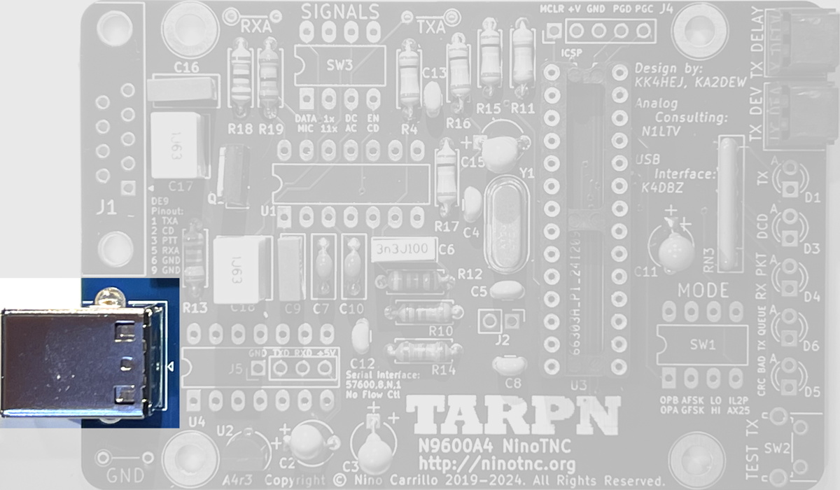
|

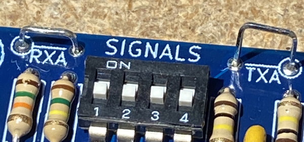
| 24 | SW1 and SW3 | 4 position dip-switch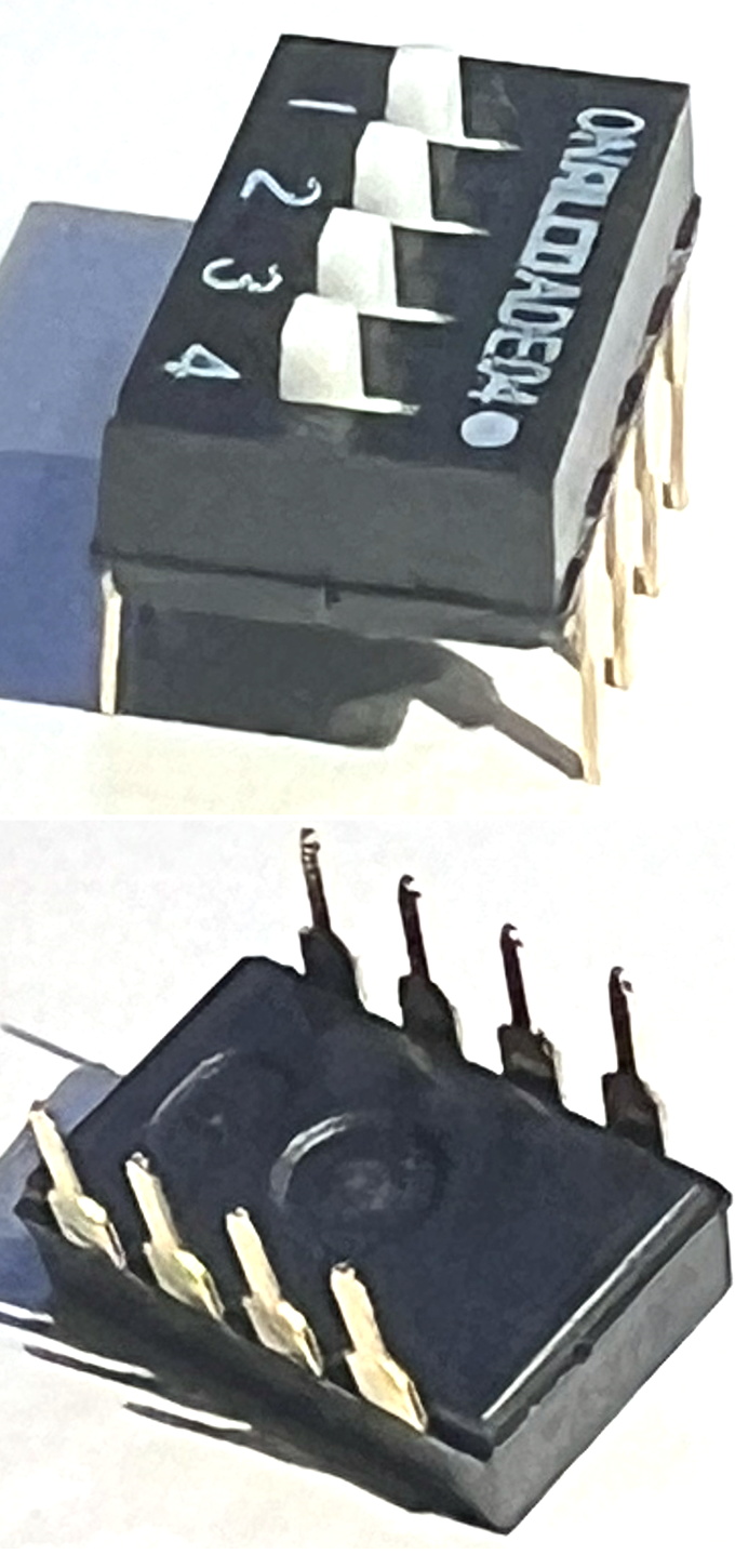
Has been black and red |
Install each switch so the label 1 2 3 4 is toward the TARPN-logo edge of the board.
Each switch is a separate circuit. SW1's four switches pull four separate CPU inputs on the CPU to VCC, and are used to select options. SW2 has four different circuits... more coming. One switch bypasses a resistor which, if the switch is off, reduces the output drive level such that a microphone input radio can be used. Important: If the switch is installed upside down, all of the photo references and instructions will be backwards. Take care in installing the swiches so the label 1234 is upright from the perspective of the TARPN-logo! 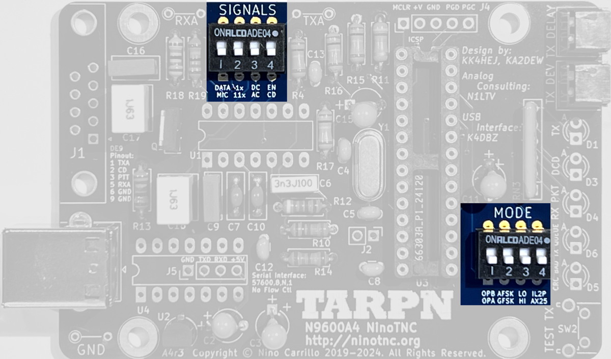
Switch SW1 controls the bit-rates and FEC mode selection. It is wired to 4 GPIOs on the dsPIC. 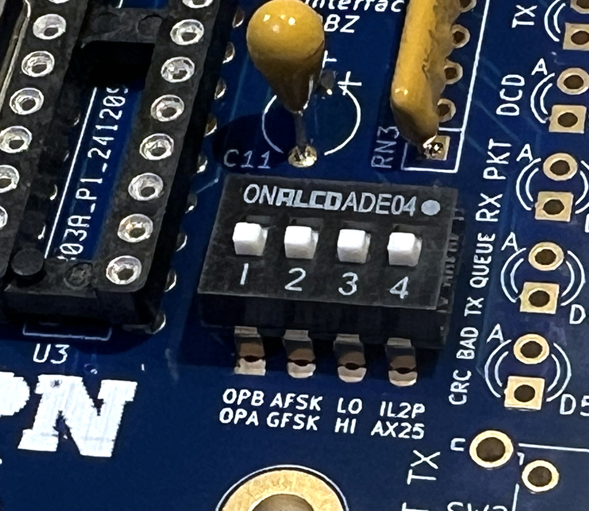
Switch SW3 is wired into the audio circuitry and to an optional carrier detect GPIO. 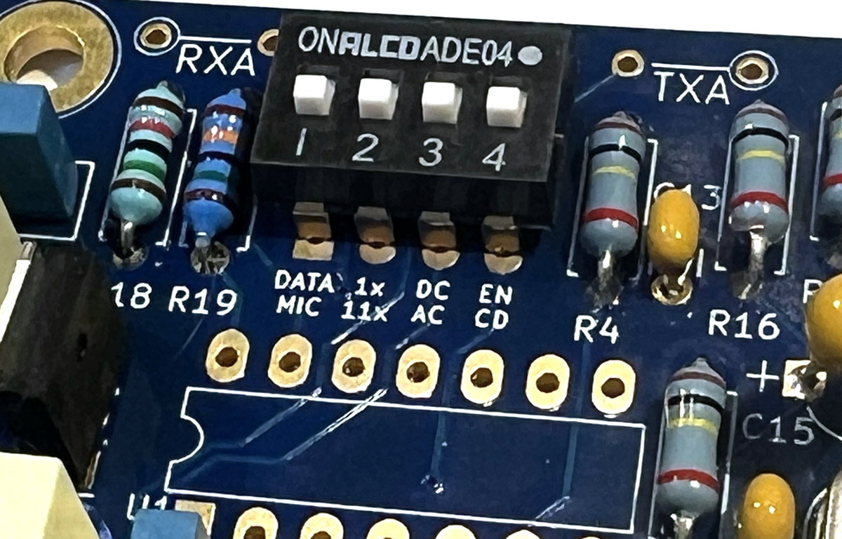
|
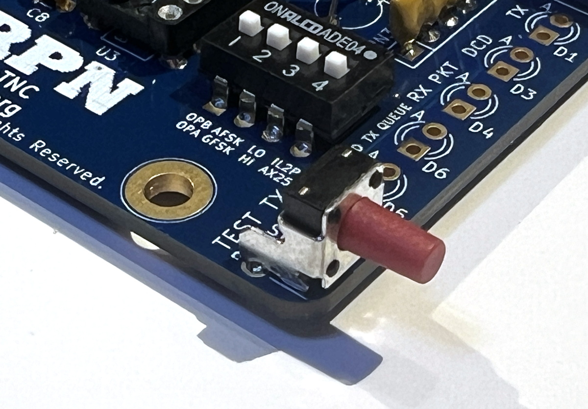
| 25 | SW2 | side facing push button switch labelled TEST TX
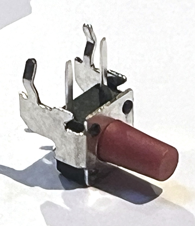 |
Mount so switch button faces off the edge of the board, directly away from the J3-pins in step 24.
Solder one of the smaller pins (not the switch shell), then, while pressing the switch into the board, wet the pin's solder again and make sure the switch is fully flush to the board.
Now solder the rest of the pins, including the switch shell, to the PCB.
This switch will tell the NinoTNC to send a transmit-audio-calibration tone and also generate a transmit packet from the saved callsign and to "CQ". The transmit packet is held until the switch is released. While the switch is held the NinoTNC will send one of 4 calibration tones which can be used for setting TX-LEV. On release, the NinoTNC sends a KISS frame back to the host with diagnostic data, and the NinoTNC also transmits the queued packet. Electrically, pressing this button connects a GPIO input on the CPU to VCC. Releasing lets the GPIO input be pulled to ground by the CPU's internal configurable "weak pulldown". 
|
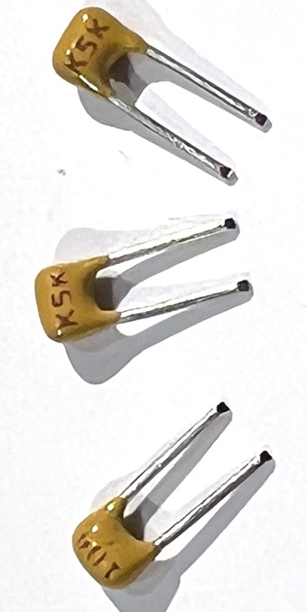
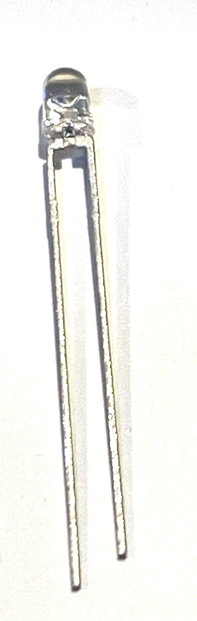
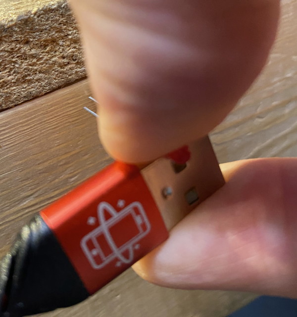
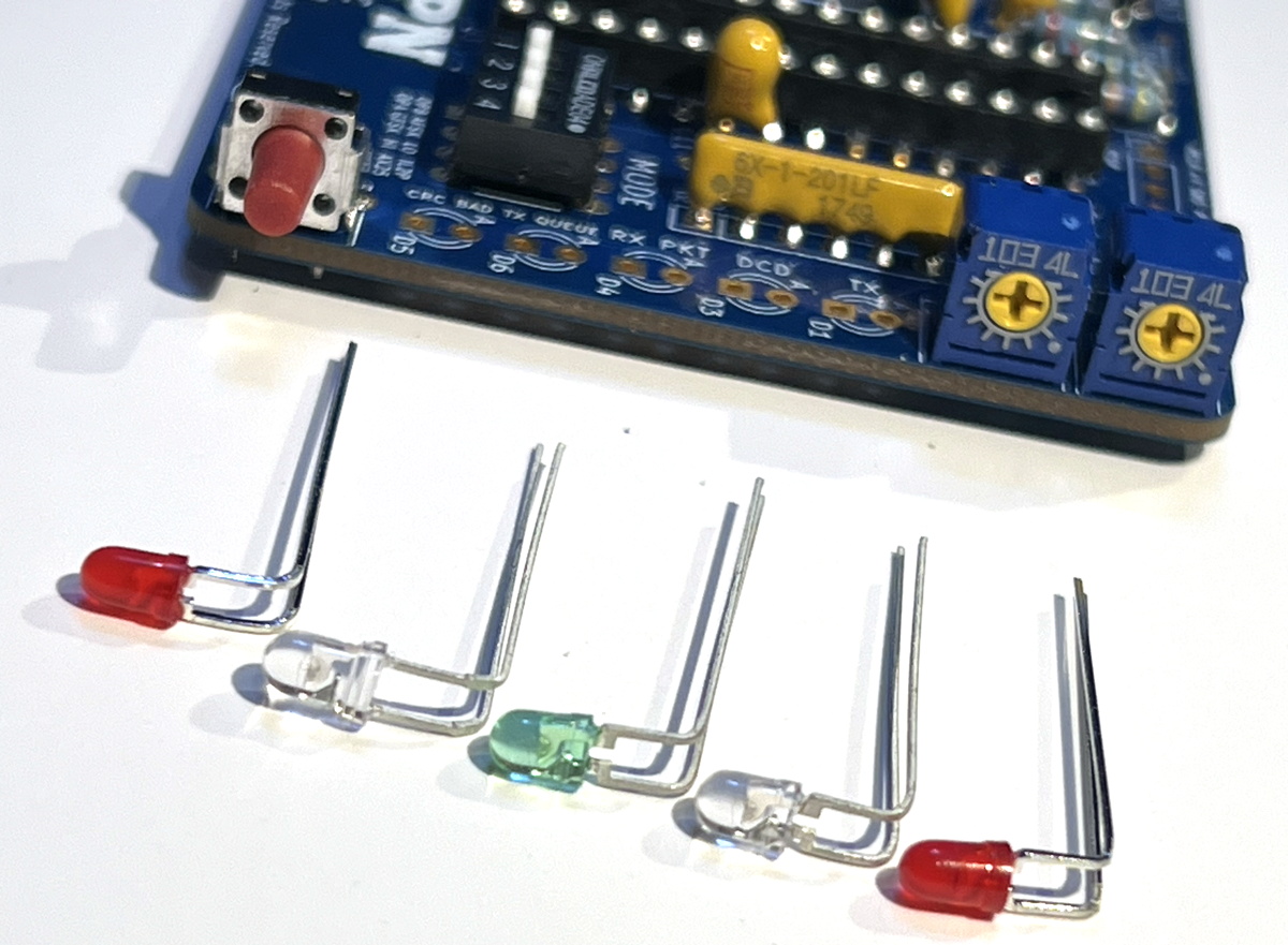
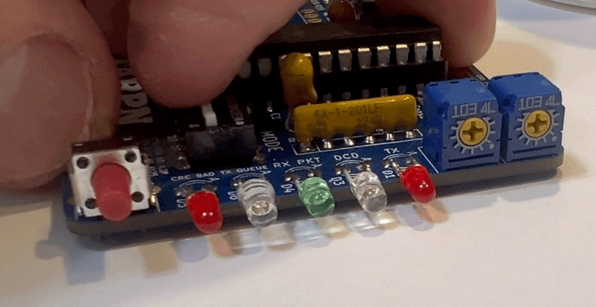
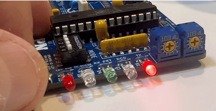
| In the next steps you'll be soldering 5 LEDs onto the PCB. When you cut the leads, save the trimmings for use as scope test loop wire in a later step. You only need 3 longish thick wire leads for the scope test loops, but save as many as you can for practice purposes. Do not confuse the clear LED with each other. The arrangement of the LEDs is important. It may be worth keeping them in their bags unit use, or tape them down on a piece of paper with the D# or color written next to them, until you bend and install the LED. |
| 26 | D1, D3, D4, D5, D6 | LED installation
Note: The yellow LED (shown here as clear) may have been substituted with a yellow-bodied LED. 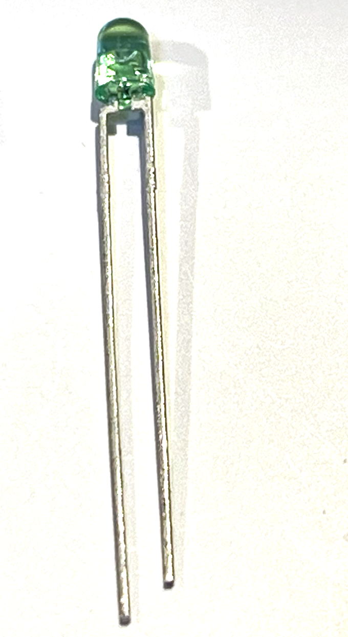
|
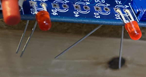
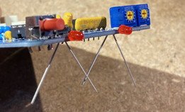
In this step you are going to bend the leads of all 5 LEDs.
What we need is a fixture to allow all 5 LEDs to be bent the same so they point out the end of the board. It is only critical that the LEDs be perfect lengths and all the same direction if you intend to ever show this NinoTNC to anybody. It's even more critical if you obtain a housing for the NinoTNC made with the LED positions in mind. The leads need to be just long enough before the bend such that the LED lays over the end of the board and just misses the end of the board. We're going to use a USB connector for a guide. It happens to be exactly the correct size. Grab a USB A connector, just like the kind on a keyboard or mouse cable where it plugs into the Raspberry Pi. Put the LED so the short lead is toward the cable side of the connector and the long lead is toward the plug. 
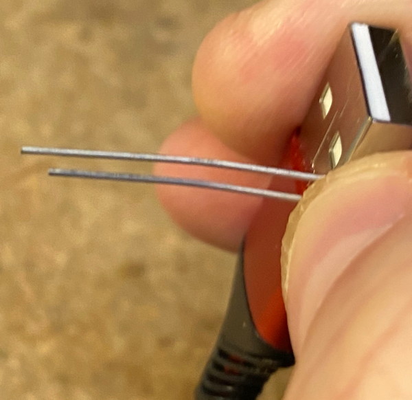
The LED body's base will be against the wide side of the plug and the wires lay around the short side of the plug. 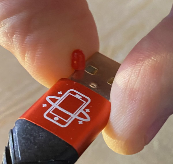
 Now fold the wires over the wide side of the plug making a 90 degree bend.
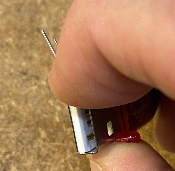
 Here is the result we want:
|
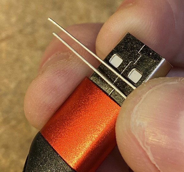
 Notice the short wire and the long wire on the LED.
The short wire goes in the hole showing the square pad.
Notice the short wire and the long wire on the LED.
The short wire goes in the hole showing the square pad.
 After bending all 5 LEDs, solder them in by color, then clip and save the trimmings for later use.
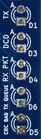 |
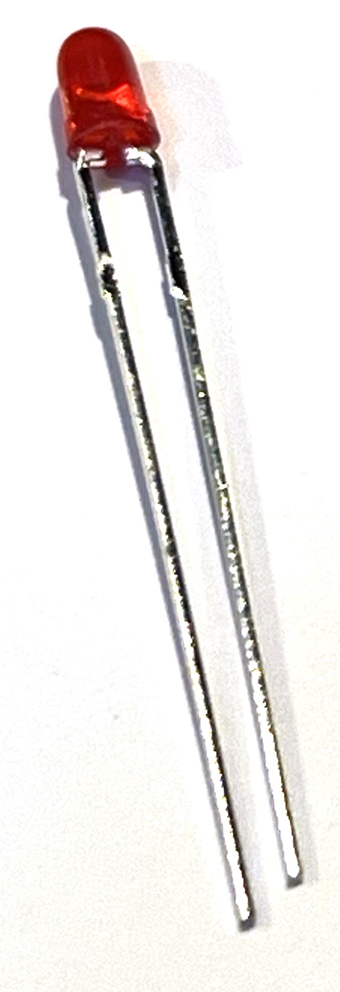
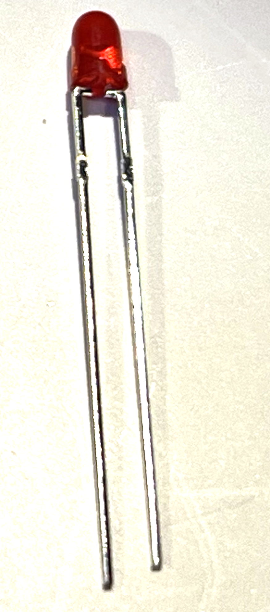
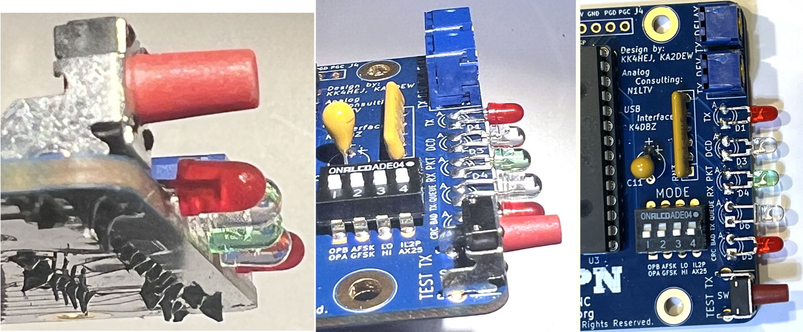
D1 | Red LED
|
TX - This LED is illuminated when the NinoTNC is keying the radio through the opto-isolator. |
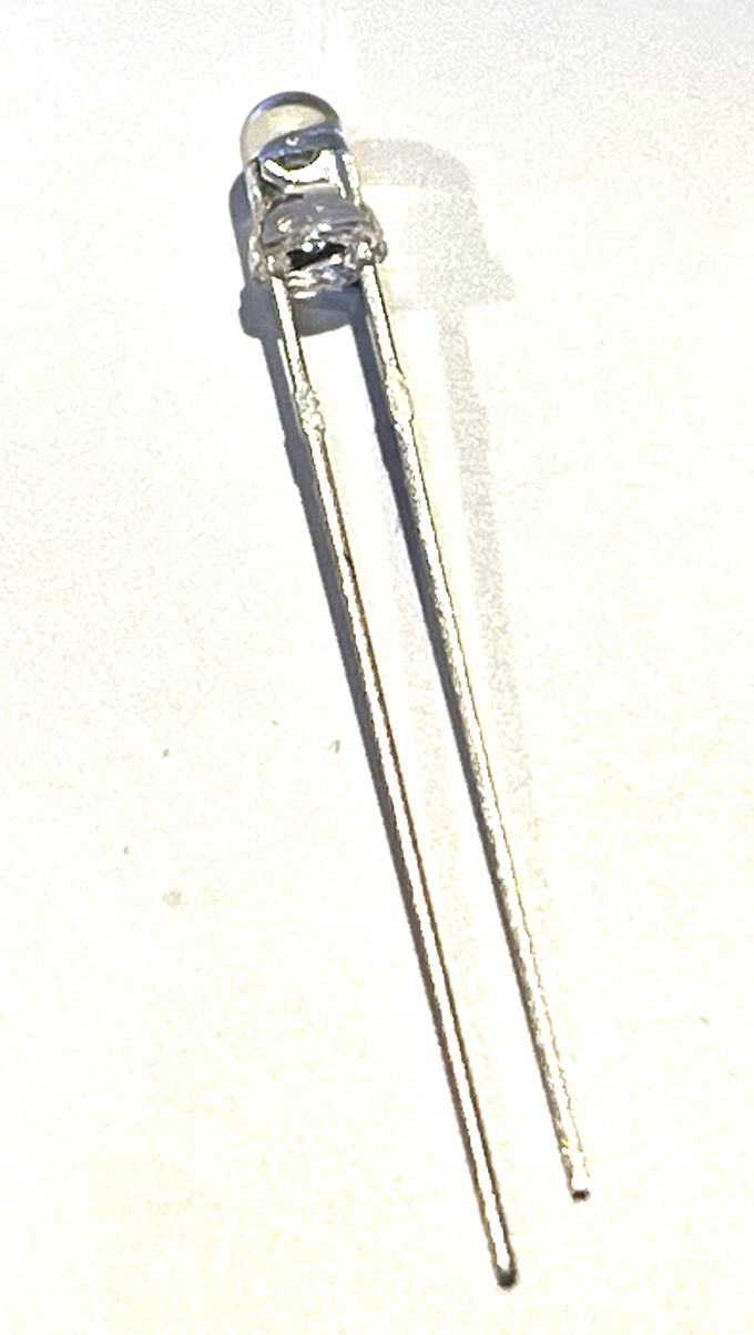
| D3 | Yellow LED
|
Data Carrier Detect. This LED will illuminate during radio received when several zero crossings occur in the wave-form (noise) which match the selected bit rate. | |
| D4 | Green LED
|
Last RX packet was decoded properly. This LED remains illuminated until a short time expires, or a packet is not decoded properly. | |
| D6 | Blue LED
|
TX message is queued. The Pending LED illuminates when the NinoTNC has a message ready to transmit but hasn't had the opportunity to get rid of it yet. | |
| D5 | Red LED | CRC error on receive packet or Receive audio at limit. When a CRC error occurs, this LED illuminates and stays on for a couple of seconds after the bad packet. When the Receive audio is at limit, the LED can flicker with the squelch noise, or will stay on if the audio stays loud. If you have receive audio control, try moving the volume high to low and see if this gives you a useful indication. Set the volume just below the point where this LED comes on. |
| 27 | U3 | Microchip dsPIC33EP256GP502 CPU
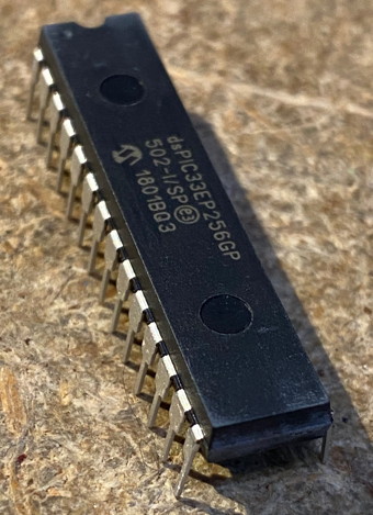 |
To make the chip fit into the socket easily, place the leads on one side against a hard flat surface and push on the package to bend the leads.
Then turn the IC over and do the same thing on the other side.
The pins themselves should be straight, but not splayed out like they are when the IC shipped.
Make sure the half moon on the IC matches the half moon on the socket and on the PCB. As you insert the chip for the first time, don't push it all the way in. 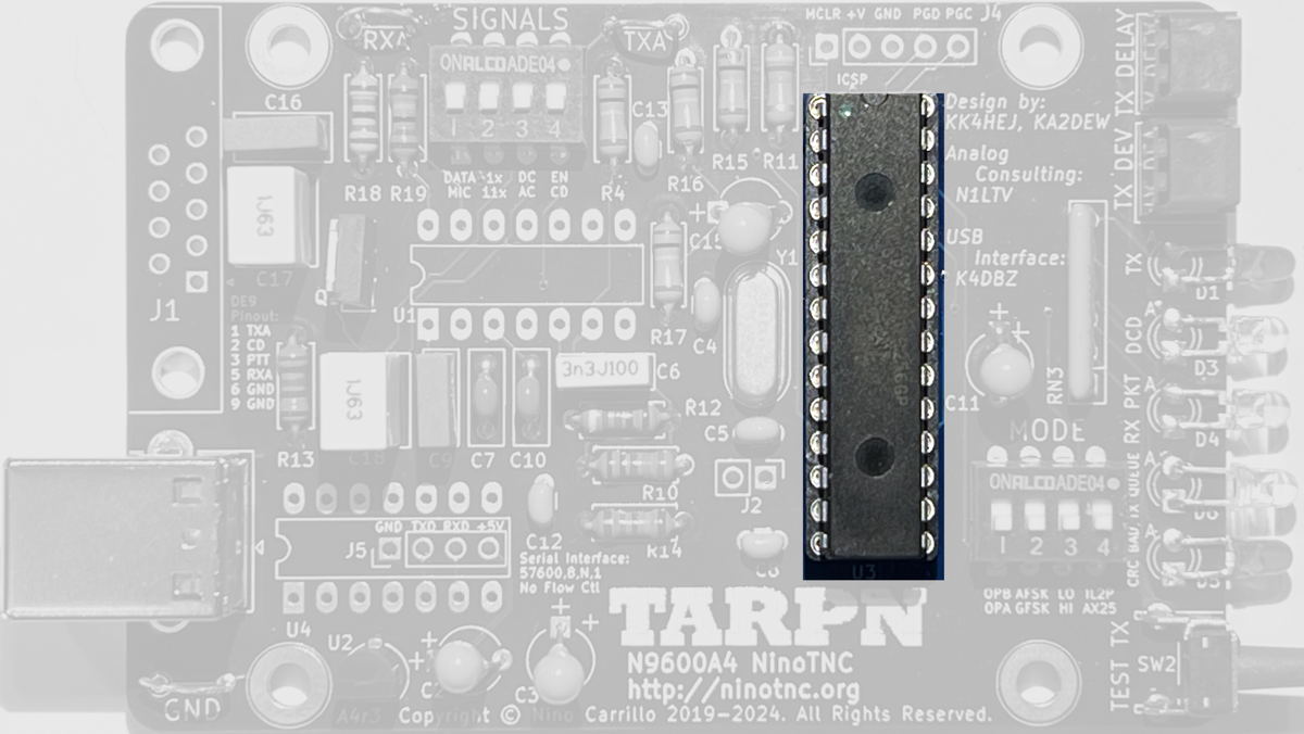
Get all of the leads to go into the 28 holes, then reverse and pull the chip back out. It may be advisable to use a screw driver to gently lift one end a little, then the other. Once the chip is removed, inspect the leads and make sure none of the bent while inserting. Fix any needing fixing and then insert the chip again, paying attention to the half-moon end as per the photo. If all goes well, push it in all the way. |
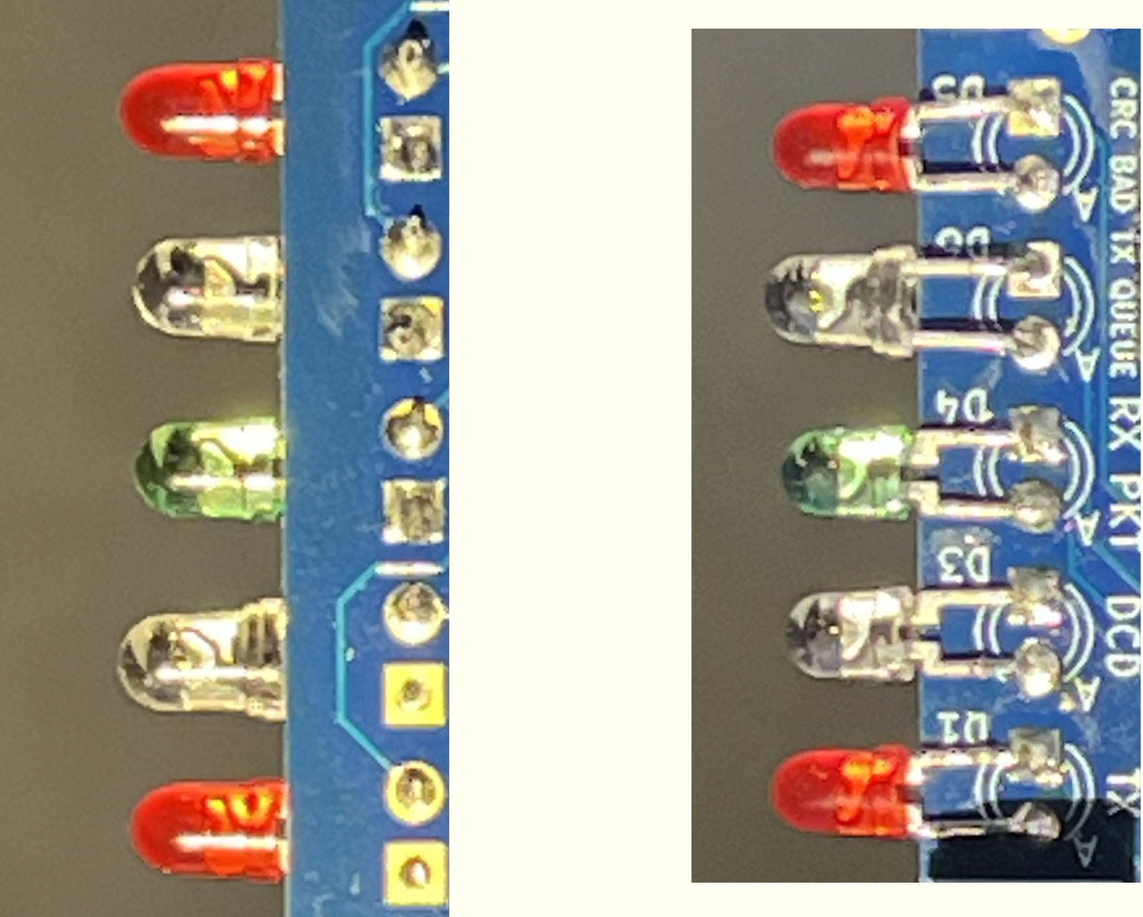 Closeup of top of silkscreen side of PCB with LED. Notice the shape of the metal inside the bulb.
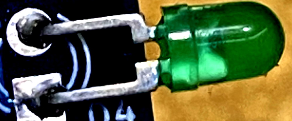 Closeup of top of back side of PCB with LED. See here that there appears to be a slot between metal pieces inside the bulb.
Now check the photos up above and see if you can tell that the LEDs match on the top photo and on the back photo.
Closeup of top of back side of PCB with LED. See here that there appears to be a slot between metal pieces inside the bulb.
Now check the photos up above and see if you can tell that the LEDs match on the top photo and on the back photo.
 If your inspection shows the LEDs are installed correctly, reapply power and use your VOM to measure the DC voltage of pins 27 and 28 of the CPU.
| 28 | Test points GND, TXA, RXA | These are loops of scrap wire bent around the blade of a long-nose-plier. 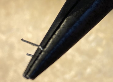 |
Test points for receive audio, transmit audio and ground.
Uses these to connect a high-impedance input audio amp to listen to packets, receive or transmit.
Or connect an oscilloscope to observe the receive voltage or wave form quality.
See pix below for installation. 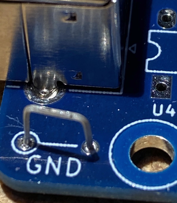
|
| The integrated circuits installed in the next two steps are exactly the same size. They are of completely different function and if you put the wrong one in, thinking you only have one to go, you will have quite a bit of work removing it! Be careful that you grab the correct chip for this next step! |
| 29 | U1 | MCP6004 quad op-amp
may substitute MCP604 or MCP6284 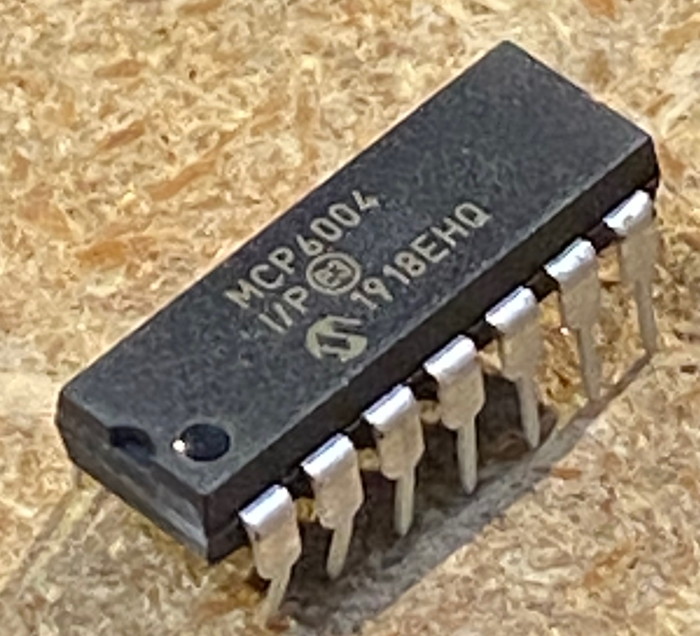 |
Install the quad op-amp Integrated Circuit without a socket.
We're not recommending using a socket for this part but only for the sake of saving a few pennies. The pins will have to be bent a little to fit. See step 27. Since the PCB is now rather crowded, and since the pin bending requirements and limits have no calibration, I recommend test-fitting the IC on the back of the PCB, and then when you get the pins bent as needed, move around to the front of the PCB and insert the op-amp where it needs to be. Make sure the half-moon shaped end lines up with the PCB. 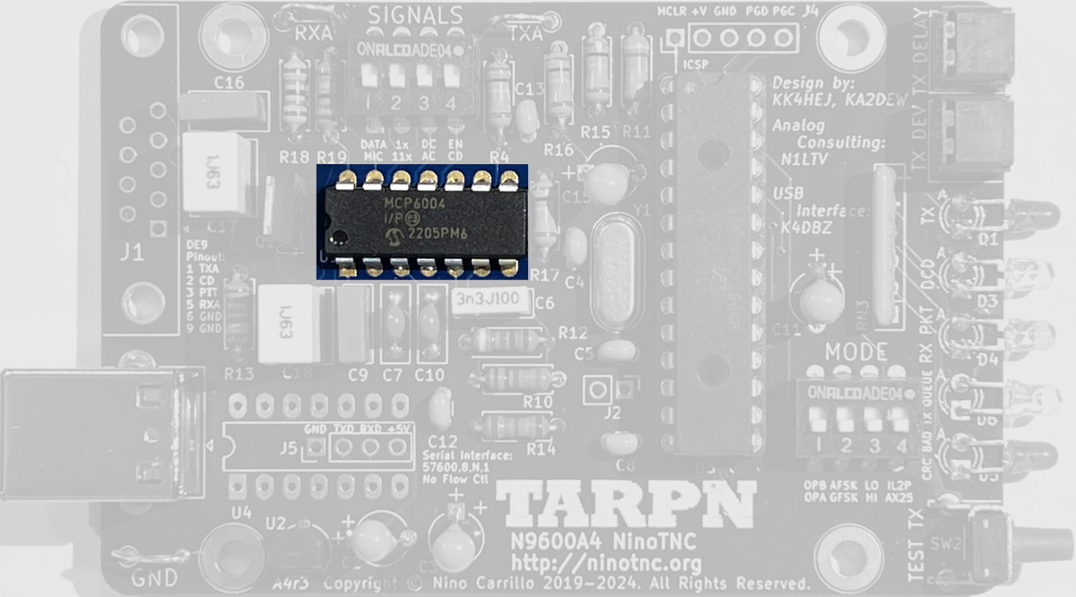
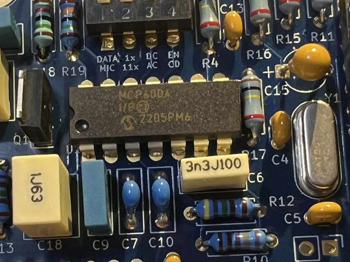 This is a quad-package op-amp (operational amplifier) used to buffer the receive AF data signal from the radio and to condition and buffer the transmit AF data signal to the radio.
The quad op-amp has 4 separate amplifier sections. One in the receive offset correction and gain stage. Two of these are used in the transmit audio shaping. One is a spare. 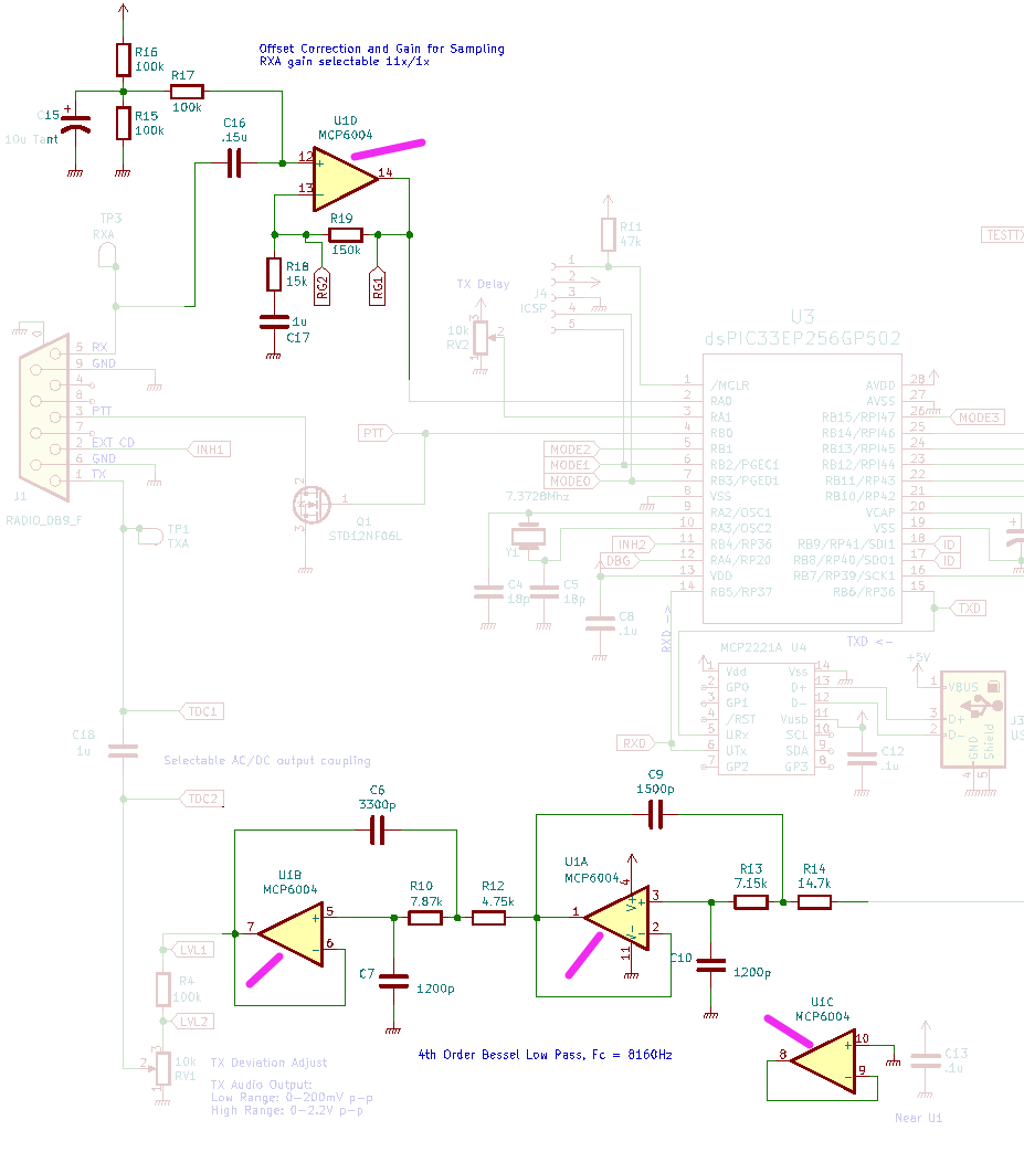
|
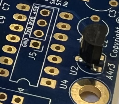
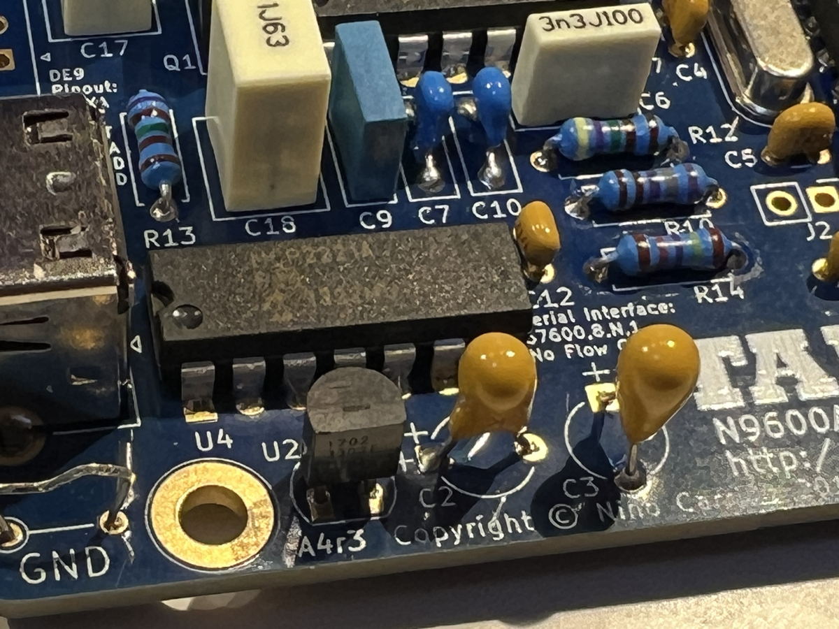
| 30 | U4 | MCP2221 or MCP2221A USB interface chip 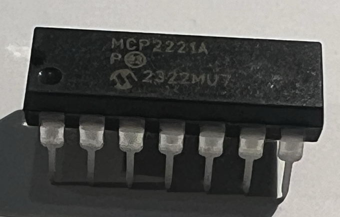 |
For USB connected applications of the NinoTNC, install the MCP2221A USB-serial interface Integrated Circuit.
Make sure the half-moon shaped end aims toward the USB-B socket. We're not recommending using a socket for this part but only for the sake of saving a few pennies. 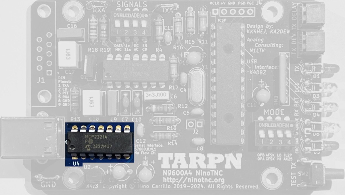
 Note the extra header pins, J5, underneath where U4 MCP2221 is installed.
These pins are for an optional header to be used if the NinoTNC will have a TTL interface and separate 5v source.
This could be handy for an embedded project where USB interconnect would be inefficient.
If you intend to use a TTL interface to the NinoTNC, don't install U4.
Note the extra header pins, J5, underneath where U4 MCP2221 is installed.
These pins are for an optional header to be used if the NinoTNC will have a TTL interface and separate 5v source.
This could be handy for an embedded project where USB interconnect would be inefficient.
If you intend to use a TTL interface to the NinoTNC, don't install U4.

|
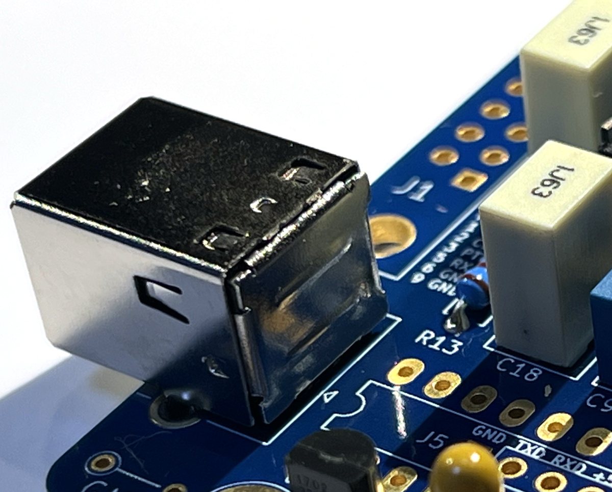
| 31 | J1 | DE9 connector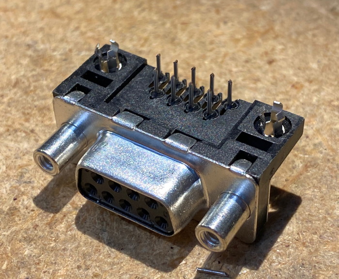 |
This connector is the interface to the transceiver from the NinoTNC.
TXA data, PTT, RXA data, and ground are connected to pins 1, 3, 5 and 6 respectively. Solder a center pin first, then squeeze the connector into the board and then reheat the center pin. Now solder the remaining 8 pins and then the two outer fingers in 3 places each. 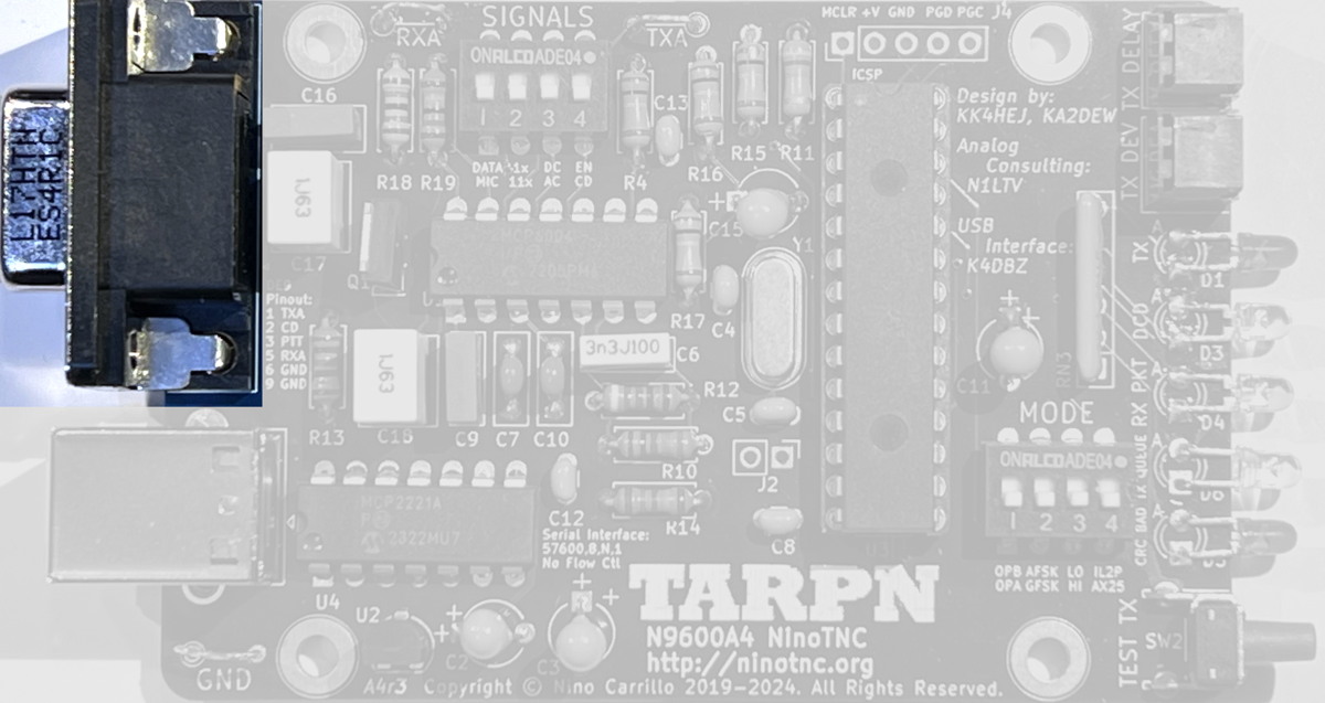 |
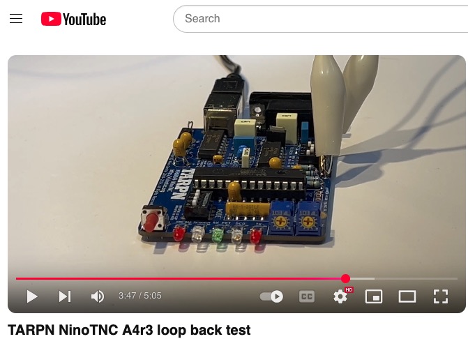 [youtube.com]
macmini:tadd$ ls -lrats /dev/*usbmodem*
0 crw-rw-rw-  1 root  wheel   13,   0 Jun 13 10:30 /dev/tty.usbmodem14601
0 crw-rw-rw-  1 root  wheel   13,   1 Jun 13 10:30 /dev/cu.usbmodem14601
macmini:tadd$
pi@raspberrypi:~ $ ls -lrats /dev/ttyACM*
0 crw-rw---- 1 root dialout 166, 0 Jun 13 10:58 /dev/ttyACM0