| home | builders | Search |
| builders ➜ TARPN Kits and Projects ➜ NinoTNC N9600A ➜ N9600A3 Assembly |

|
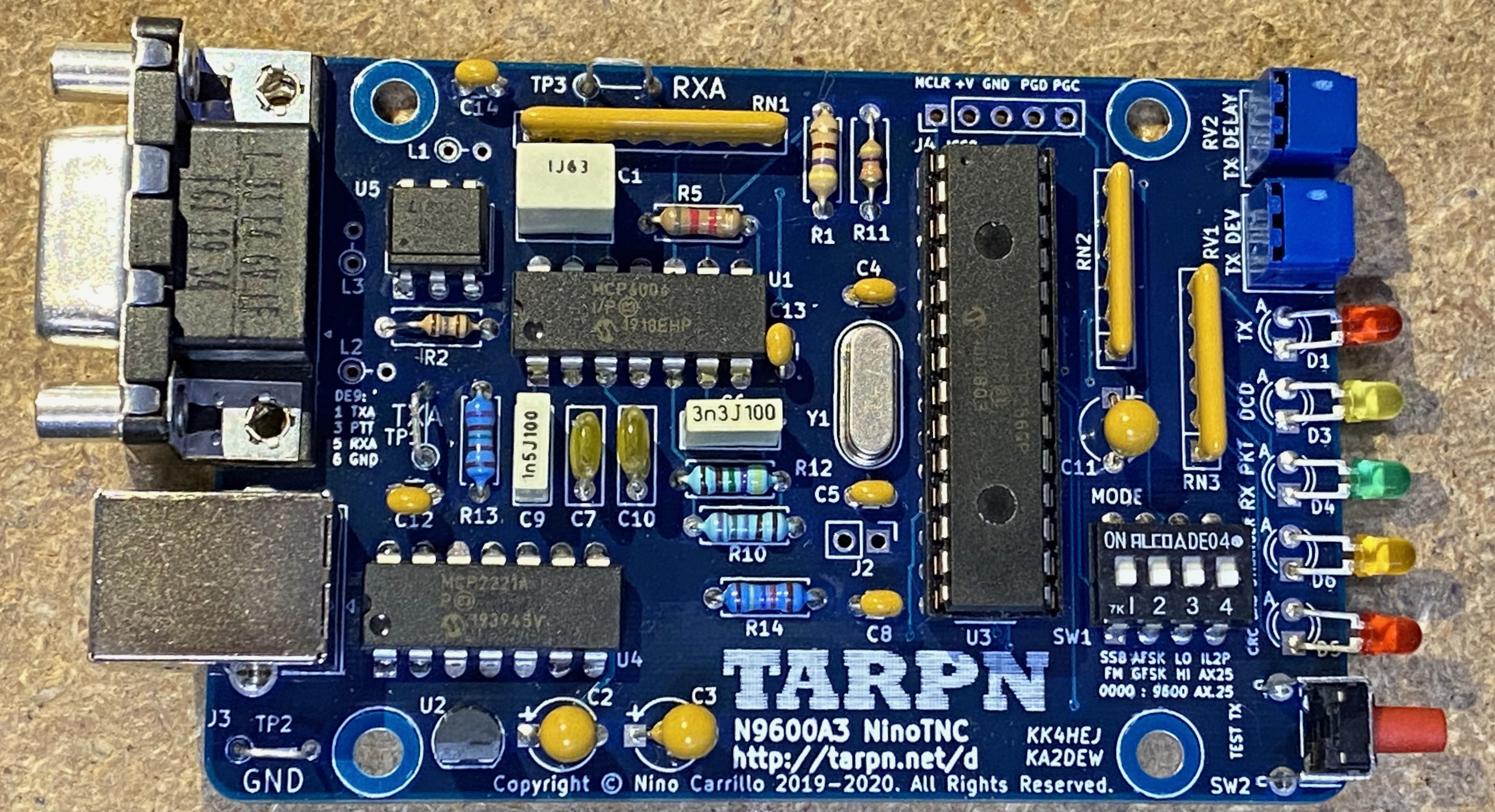
These are the assembly instructions for the N9600A3 board. Make sure the silkscreen information on the board you are assembling matches this.
The bill of materials linked below is specific to the N9600A3 board, both with and without the 'r3' mark.
There are some instructions specific to the 'r3' and others for the prior 'r2' boards.
Only the 'r3' board is specifically marked.
The differences between the two boards are in the installation of resistor R12 in step 7, and jumper J6 in step 20.
Additionally capacitor C12 is in a different location in step 9.
|
|
| Bill Of Materials |
Right-click on this link and save the n9600a3 bom csv file to your computer.
This is the Digikey shopping list for the TNC. Find the n9600a3 csv file on your computer (it will be named starting with n9600a3 and will be a csv, comma separated values, file) |
|
| Go to Digikey website | Click on this link: Digikey |
|
| Shopping Cart | Click on the shopping cart. If presented, click on View Cart button. |

|
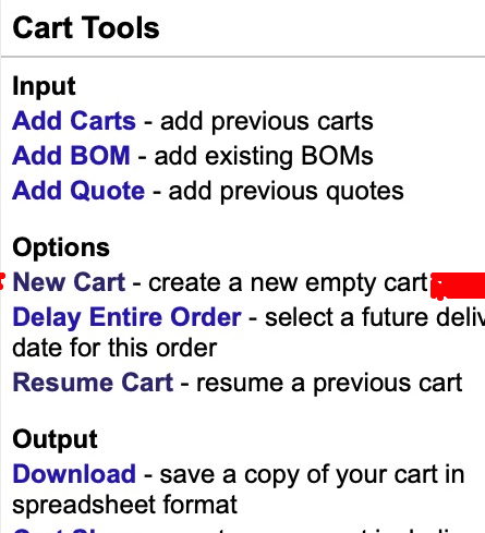
| New Cart |
if there is no New Cart button, skip to Upload CSV, else click the New Cart button. |
|
| Upload CSV |
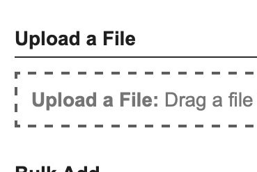
There is an Upload A File field in the middle of the form.
Drag the CSV file from your Finder/Explorer into that field, or click on the Browse link, and then navigate to the CSV file. |
|
| Confirm Mapping |
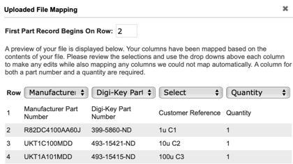
You will see a pop-up window titled "Upload File Mapping".
Find the titles (in row 1) on that window and make sure the column headers match the text in the title row. Make sure the third column ROW drop-down says "Customer Reference". Click on Add To New Cart |
|
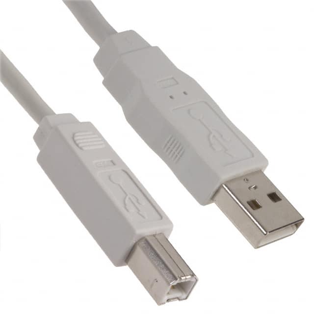
| USB cable? |
If you need a USB A male to USB B male cable, add it now.
Part# WM21039-ND is $2.16 for a 3'4" cable. There are suppliers of 1 foot USB-B cables at other vendors (Amazon). Short is better for RF immunity but it does have to make it from the host computer (Raspberry Pi) to the NinoTNC. |
|
| Checkout |
Inspect the list. If anything is backordered, stop and send an email to [email protected] email reflector.
Almost everything is available from a second source right on Digikey. We'll fix it and send a reply.
If you go ahead and let it be backorded, DigiKey will charge you postage twice.
Now do checkout and pay for your order. Shipping: USPS shipping is the cheapest. Paypal works. |

|
| ⇒ All parts are inserted from the silk-screened side of the board, i.e. from the side on which the white writing is printed. |
| ⇒ Except where specifically noted, all two pin components are non-polorized so you can put the part onto the board with the pins in either hole. |
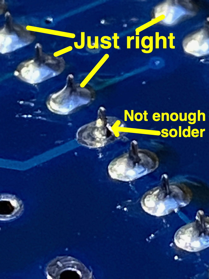
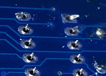
 Inspect the leads to make sure the solder comes up over the lead for a visible amount.
Cut the lead at the wire, not the solder.
The solder is your friend.
What you do NOT want is a lead which is not making good electrical contact with the hole.
Inspect the leads to make sure the solder comes up over the lead for a visible amount.
Cut the lead at the wire, not the solder.
The solder is your friend.
What you do NOT want is a lead which is not making good electrical contact with the hole.
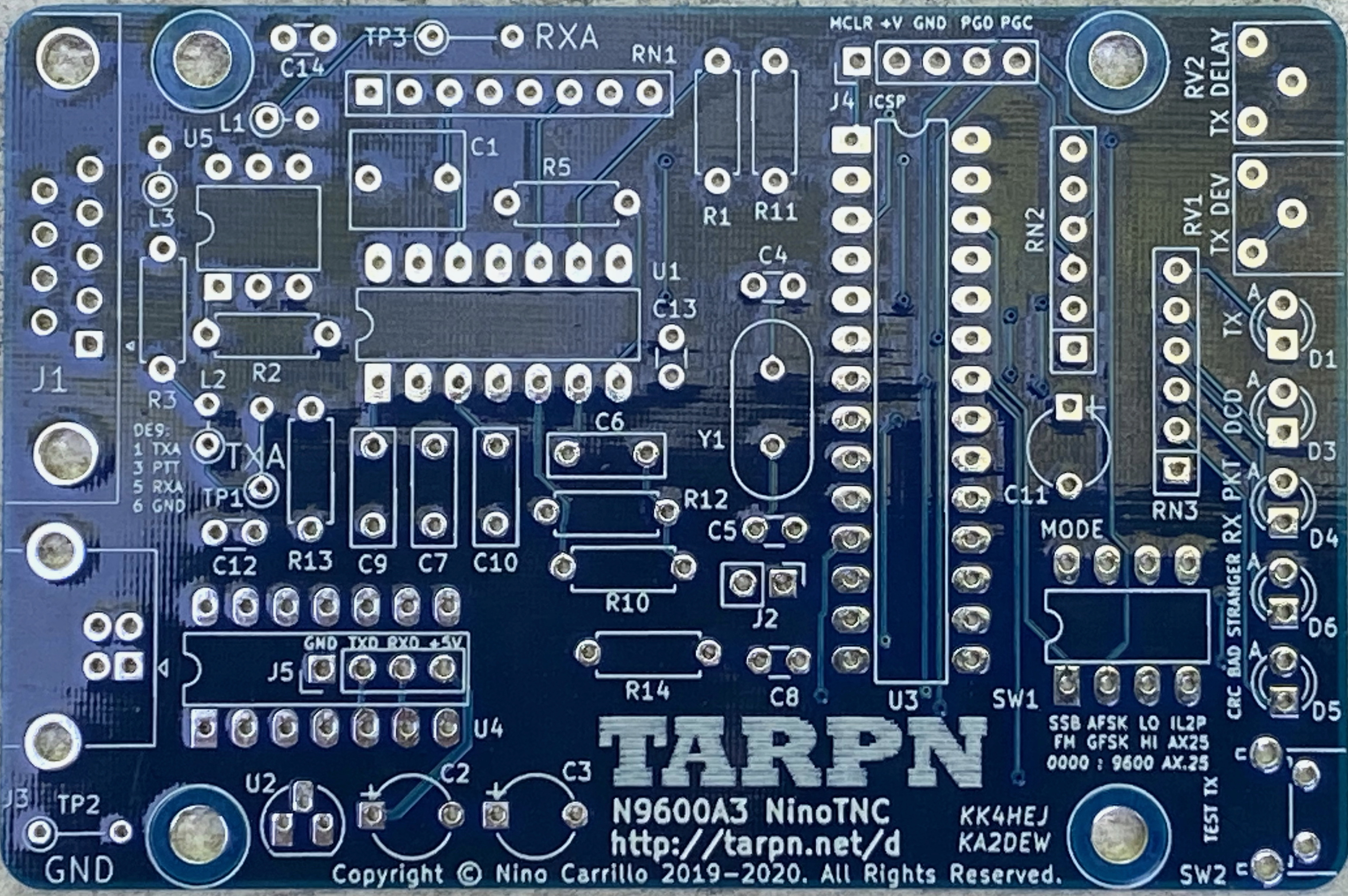
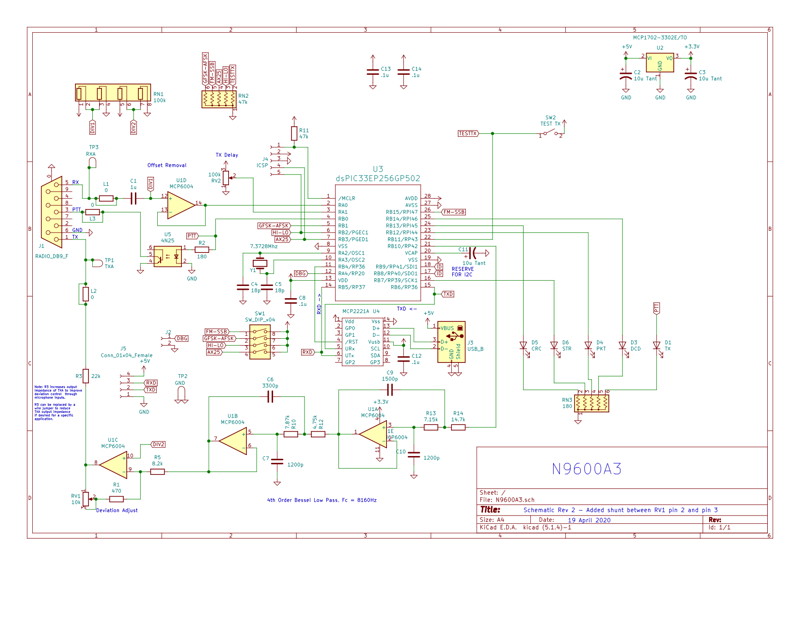
 A3 rev r3 board:
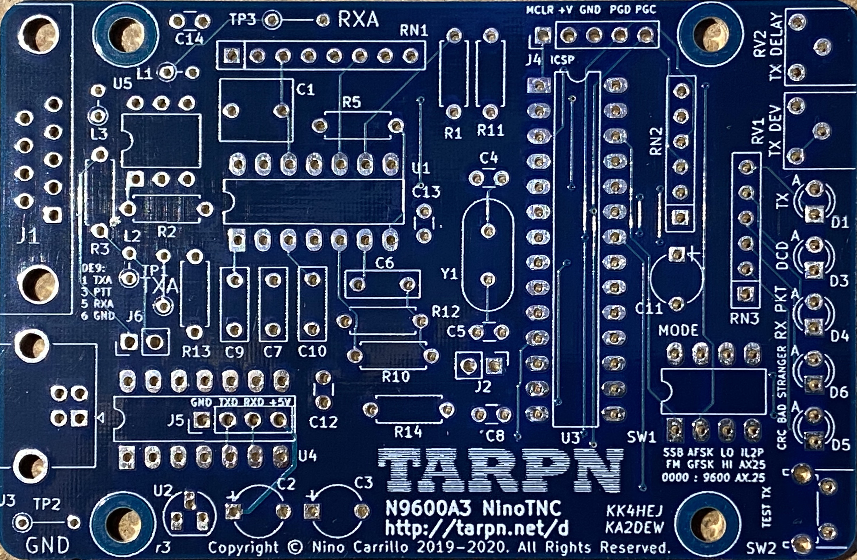 Here's the A3 rev r2 PCB's schematic. Click to load the PDF.
| 1 | Y1 | 7.3728 MHz crystal
 |
The crystal will have some lettering on it containing the numbers 7.37
The crystal and two capacitors form an oscillator to provide clocking for the CPU's digital circuits. 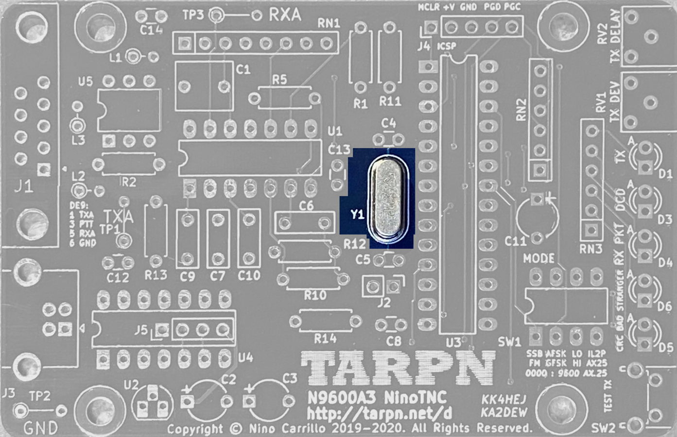 |
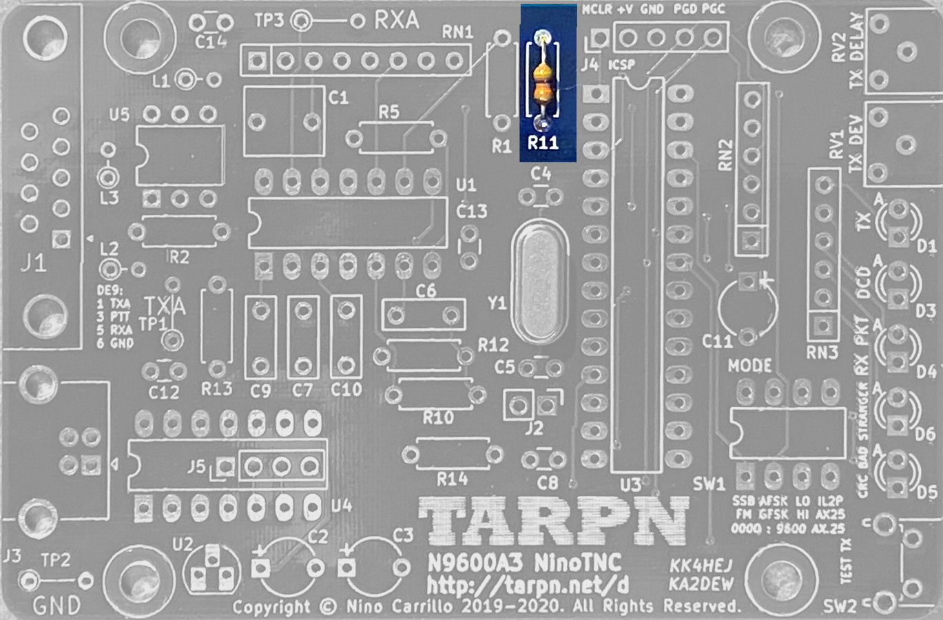
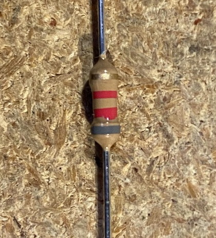
| 2 | R11 | 47 kΩ 5% 1/4 W resistor
|
R11 turns off the MCLR input to the CPU.
|
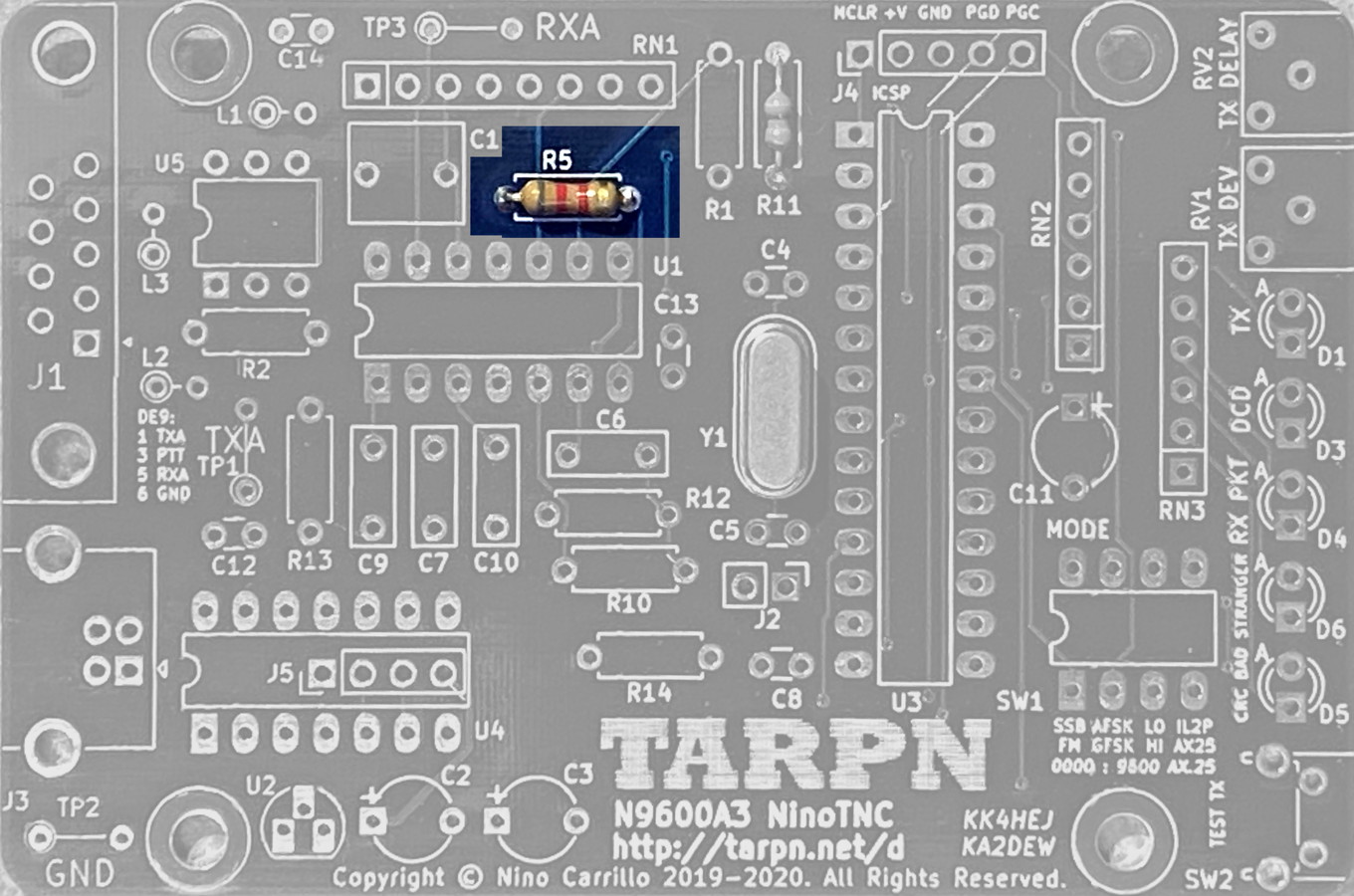
| 3 | R5 | 8.2 kΩ 5% 1/4 W resistor
 |
In the TX-data/audio path between U1B and U1C op amp devices.
 |
| 4 | R1 | 470 Ω 5% 1/4 W resistor 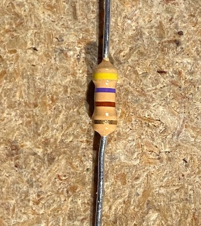 |
This is a low-end-limit to the Deviation adjust. 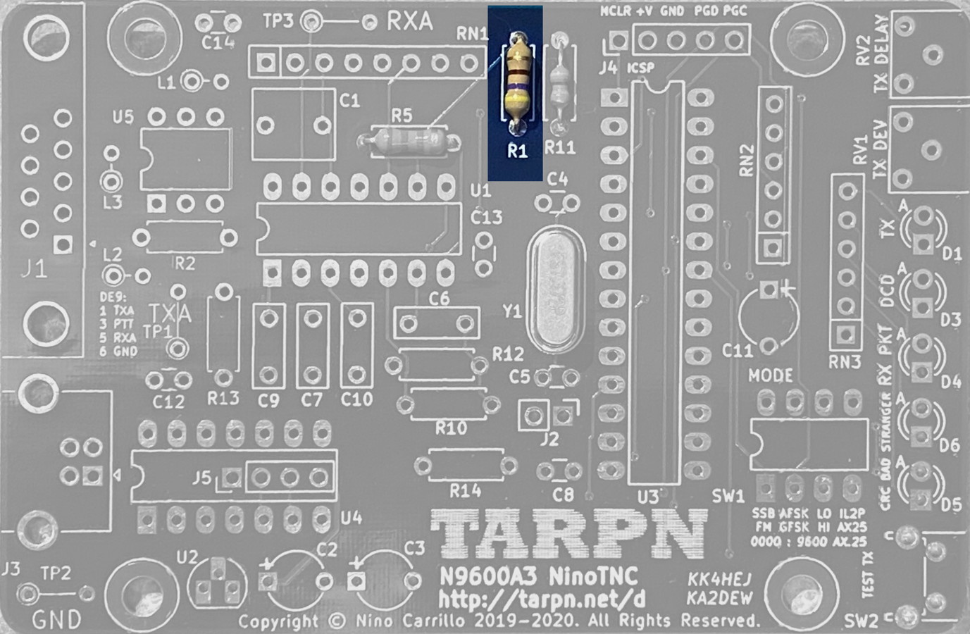 |
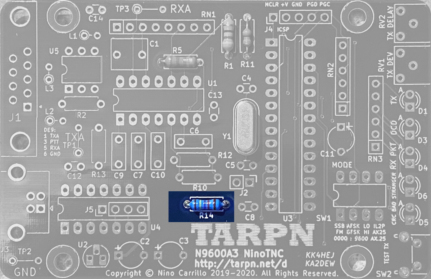
| 5 | R14 | 14.7 kΩ 1% 1/4 W resistor 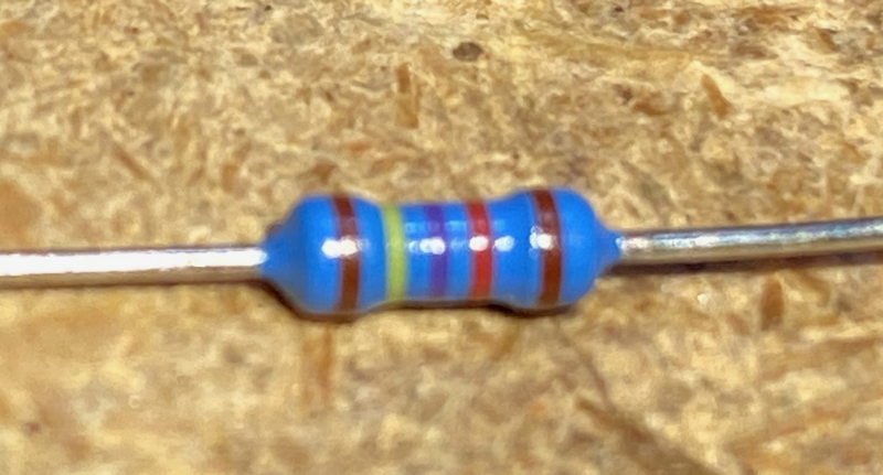 |
This is part of the amplifier circuit for the 1st op-amp stage in the transmit data circuit.
 |
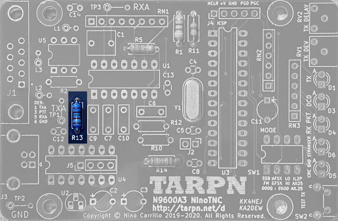
| 6 | R13 | 7.15 kΩ 1% 1/4 W resistor 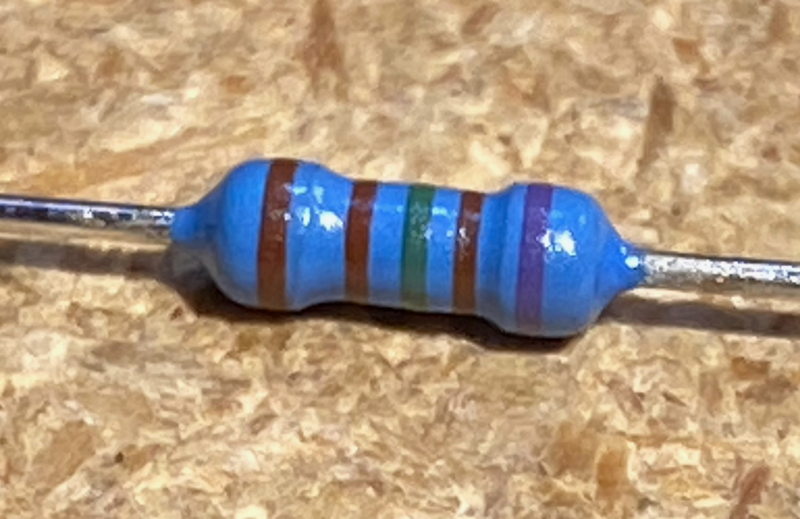 |
This resistor is in the input and feedback loop for the 1st op-amp stage in the TX-data/audio path.
 |
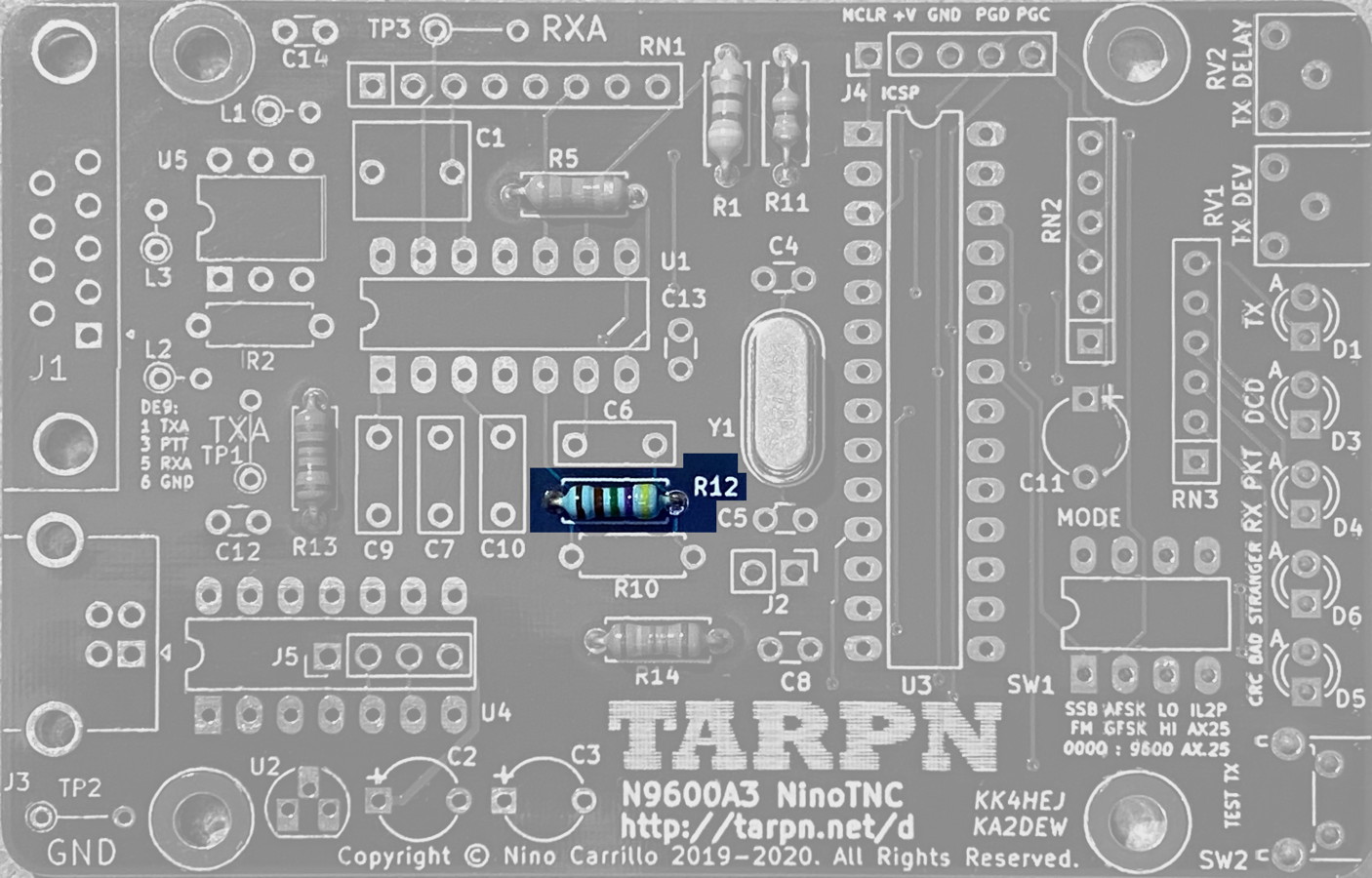
| 7 | R12 | 4.75 kΩ 1% 1/4 W resistor  |
This resistor is in the audio path between the 1st and 2nd op-amp stage in the TX-data/audio path.
 |
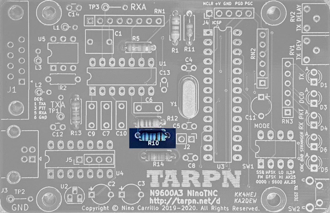
| 8 | R10 | 7.87 kΩ 1% 1/4 W resistor 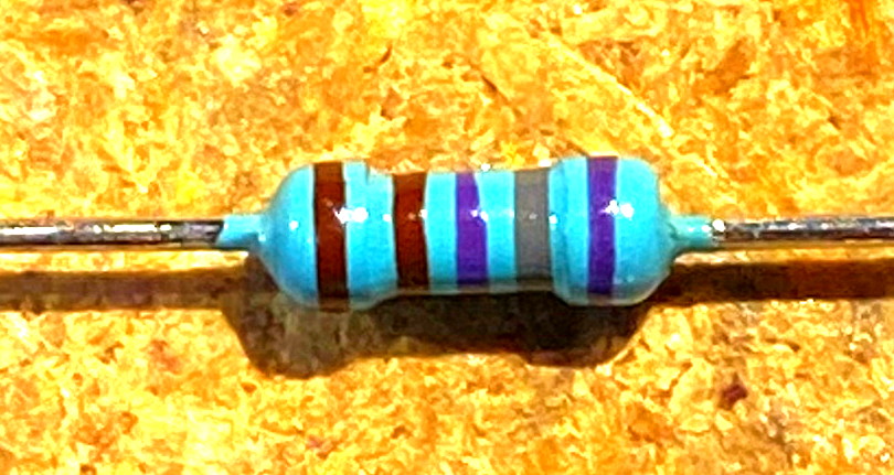 |
This resistor is in the input and feedback loop for the 2nd op-amp stage in the TX-data/audio path.
 |
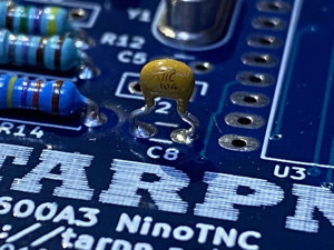
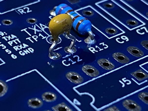
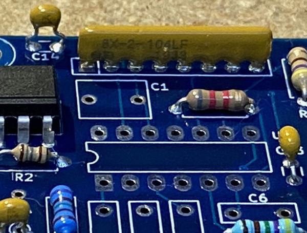
| 9 | C8, C12, C13, C14 | 0.1 µF 10% 50 V Ceramic capacitor 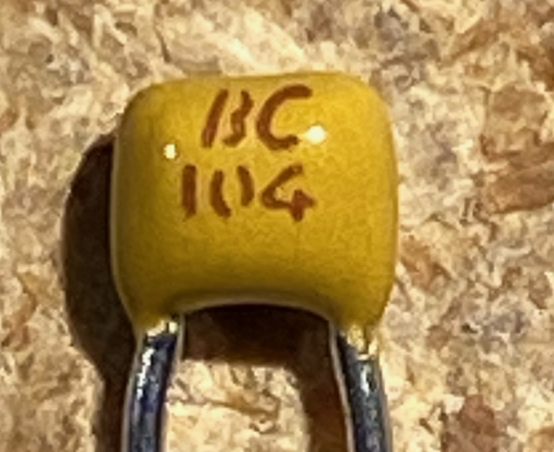 |
These ceramic radial capacitors provide power supply filtering and glitch reduction on the CPU’s main power input and at 3 other places around the board. .
Note: C12 is half an inch to the right of where pictured for boards marked with 'r3'. 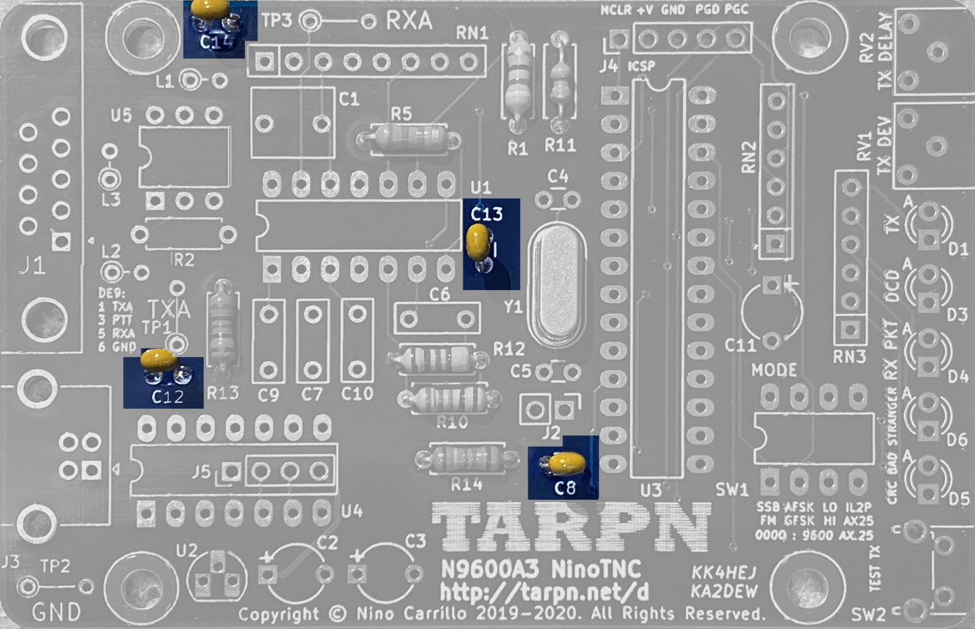 |
 |
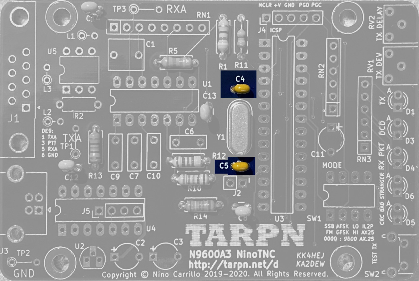
| 10 | C4 and C5 | 18 pF 5% 50 V Ceramic capacitor (may be 100 V)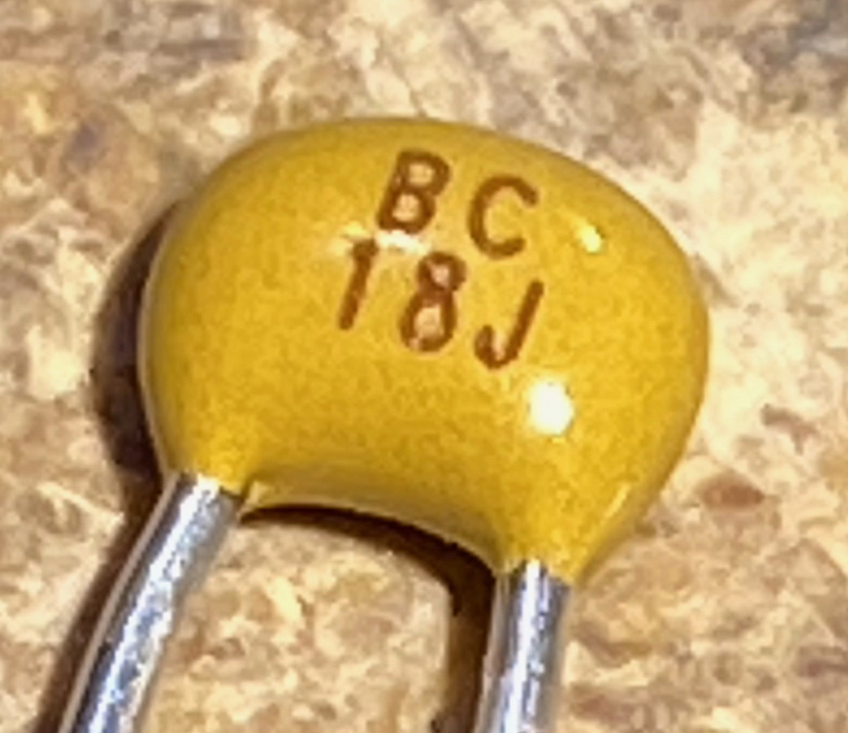 |
C4 and C5 are part of the crystal oscillator circuit
 |
| 11 | R2 | 180 Ω 5% 1/8th W resistor |
R2 is the current limit resistor between the GPIO and U5, optoisolator.
|
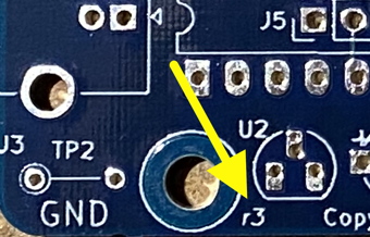
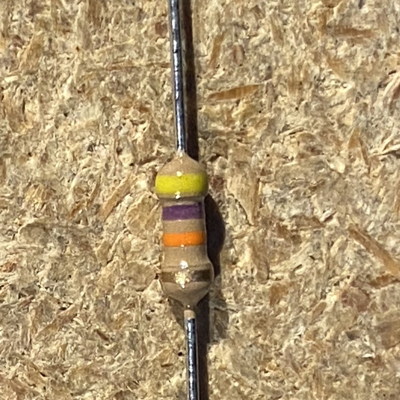
| 12 | R3 | Follow blue text for 'r3' boards and green text for the 'r2' board. r2 board: install bare wire or 22 kΩ 5% 1/2 W, 1/4 W, 1/8 W resistor r3 board: install RES 22 kΩ 1/4 W 5% AXIAL 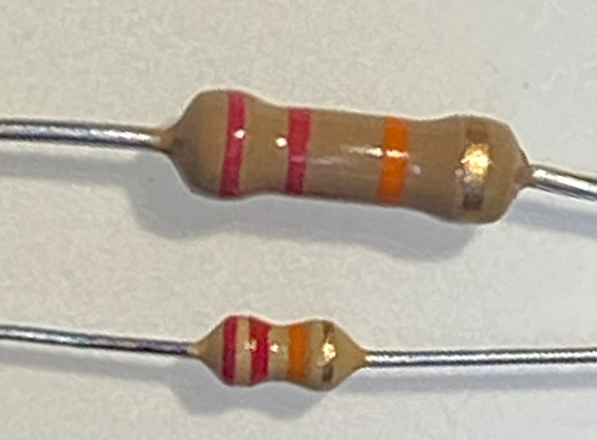 1/2 W and 1/8 W shown |
This instruction is especially confusing because the part we're talking about goes into a position silkscreened with Resistor 3 parts designator R3, and the different behavior is keyed off a mark on the board which is 'r3' (lower case).
The R3 position on the PCB is in the transmit audio circuit after the last op-amp.
When in circuit, R3 reduces the TXA level into the range of voice radio microphone input.
For older r2 boards (not labelled), only install this resistor if you are going to use the TNC to drive data into the microphone input of a transceiver in 1200 baud service. This value could be higher than 22 kΩ so keep that in mind if you need to do a field install of the resistor at a later date. Up to 82 kΩ is probably fine. You'll know if you can't get the TX Level high enough or low enough. You're goal is to get the TX level to be adaquate to get a low failure rate to the other end of the link. For other than a series 'r3' board, this resistor must be replaced by a bare wire for digital radio operation because the resistor creates minor distortion in the audio which cannot be permitted at 4800 or 9600 baud. One hack might be to install this resistor and then install a thin wire on the bottom of the board shorting the two ends of the resistor. For 'r3' board, marked next to the lower left screw, always install this resistor. 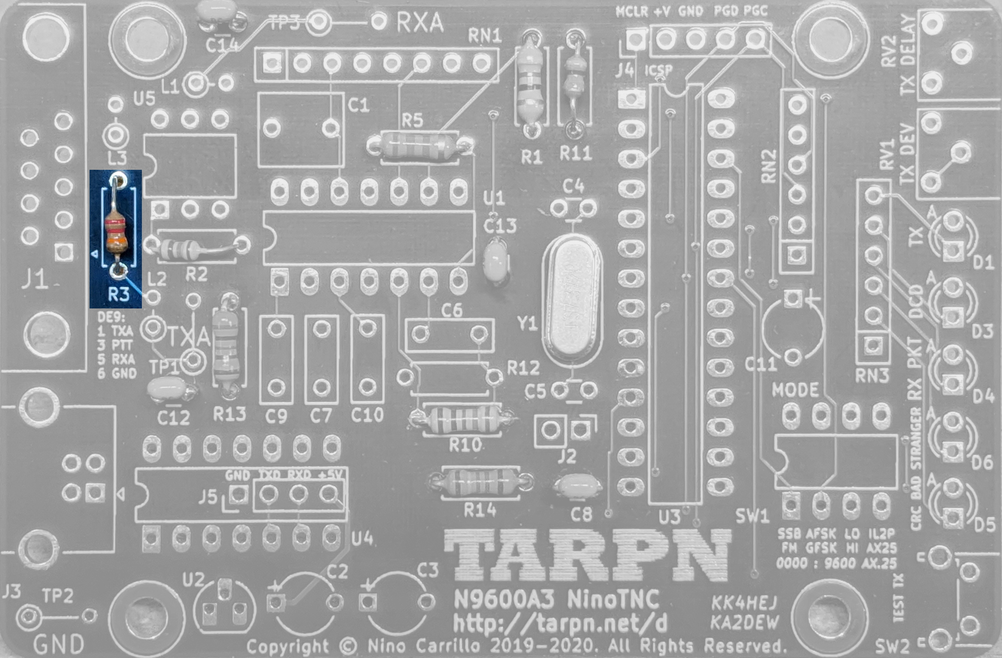 |
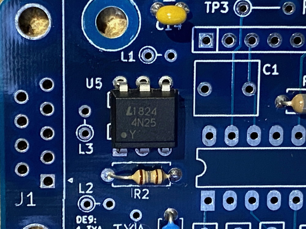
| 13 | U5 | 4N25 iso-optilator PTT driver.
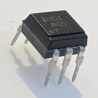
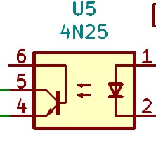 |
Install so the pin 1 dot on top of the part is toward the half-moon on the PCB.
This six-pin device is driven by a GPIO on the CPU and is responsible for pulling the PTT line to ground when the NinoTNC wants to send a packet. If this part is missing, dead, or inserted incorrectly, the TX LED on the TNC will still light, but the radio will not transmit. An opto-isolator uses an internal light source to charge the optically sensitive diode which allows energy to pass. This sealed package performs the duties of an open collector transistor but with a major feature that no energy at the collector can pass back to the gate/base. Consult the schematic diagram. Pin 6 is left disconnected. Pin 3 is a no-connect. Pin 1 is driven by the CPU pin 4 GPIO through a 180 Ω resistor R2. Pin 2 and 4 are tied to ground. When P1 is raised high, the internal LED illuminates the transistor between pins 4, 5, and 6, causing pin 5 to pull to near ground, keying up the attached radio. In a traditional TNC, the CPU drives the transistor through a resistor but if the transistor is not driven, the PTT pull-up voltage at the transmitter can leak back through. This is of no consequence if the CPU is powered up. However, if the CPU is powered off, and the radio is on, the radio can actually provide enough energy leaking through the PTT circuit to activate the CPU. The CPU will then start its boot up procedure, possibly reading control inputs (which are powered down) incorrectly. The opto-isolator prevents the PTT leakage from getting to the CPU because there is no route backwards through the LED. 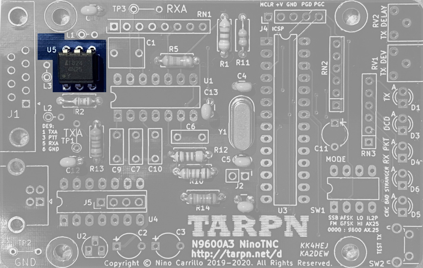 |
 |
|||
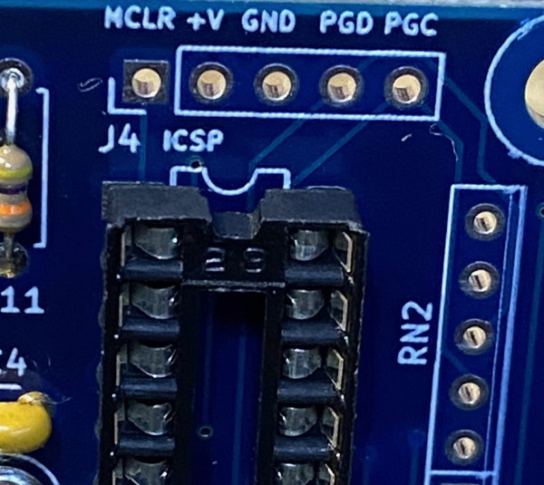
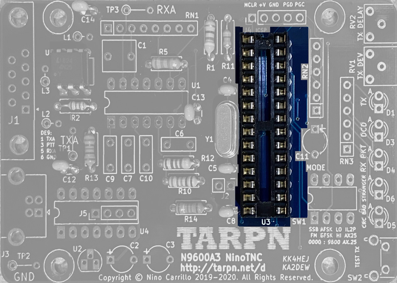
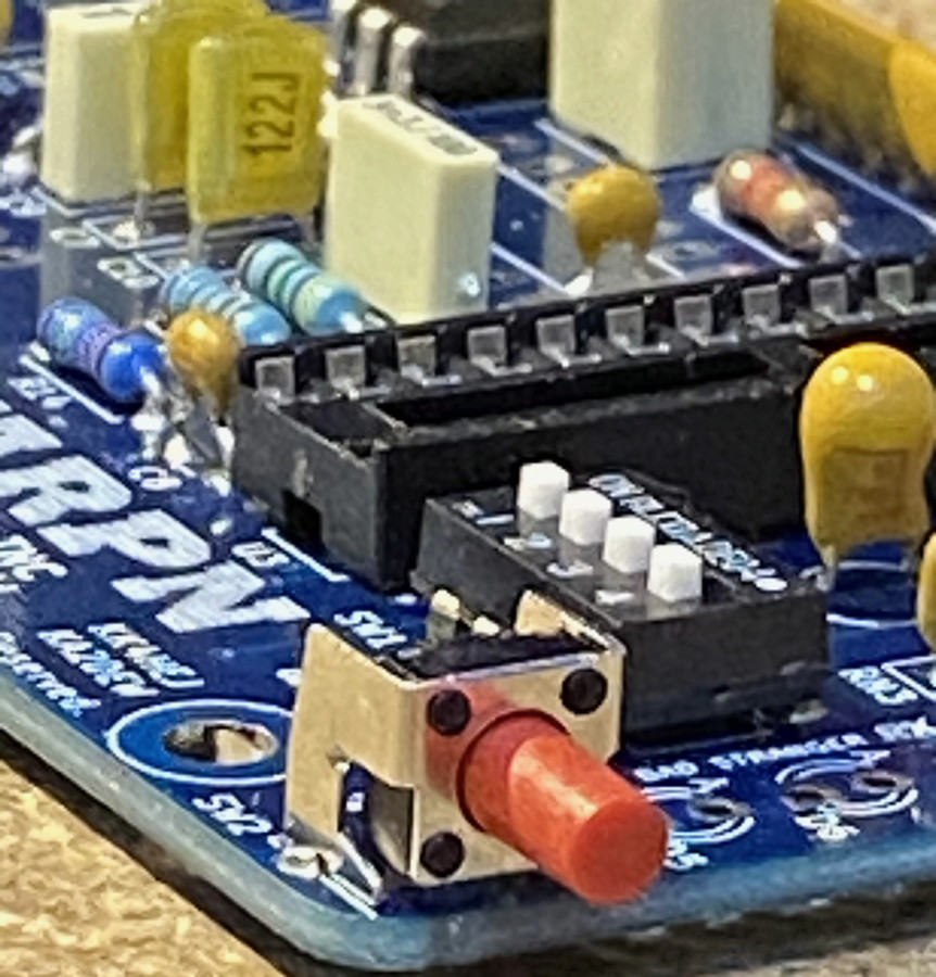
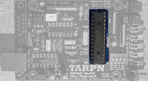
| 14 | XU3 | 28 pin DIP IC socket for U3
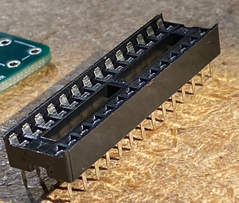
| This is the socket for the CPU.
 |
| 15 | U2 | MCP1702 3.3 V 250 mA TO92 case regulator 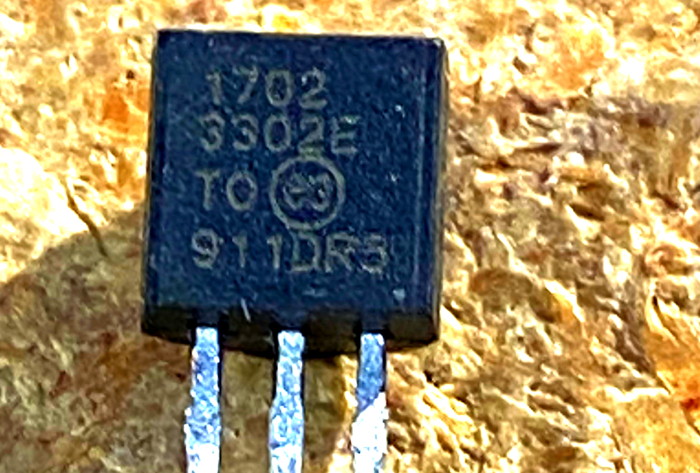 |
This part takes the 5 V DC from the USB connector and regulates it down to 3.3 V, as needed by the CPU.
Align flat edge with the board silkscreen  |
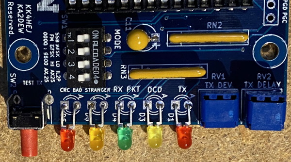
| 16 | RN1 | 4 resistor resistor network.
Could be 56 kΩ or 100 kΩ 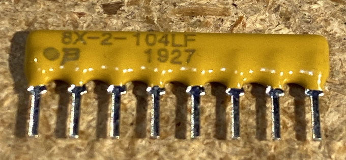
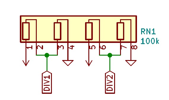
Note: Text on the part itself could be different because 56 kΩ or 100 kΩ is suitable. |
Orientation is important!
Pin 1 is identified by the square around the hole on the PCB and an interesting symbol near the end pin on the component. See schematic symbol below. If you are looking at the print on the one side of the resistor pack such that the pins are down, then pin1 is on the left. This part serves as a pair of resistor voltage dividers. The first follows the input audio coupling capacitor so the voltage of the RX audio is centered around 3.3v/2. The second is used to provide a bias to the C element of the MPC6004 quad op-amp package in the final stage of the TX audio shaping. 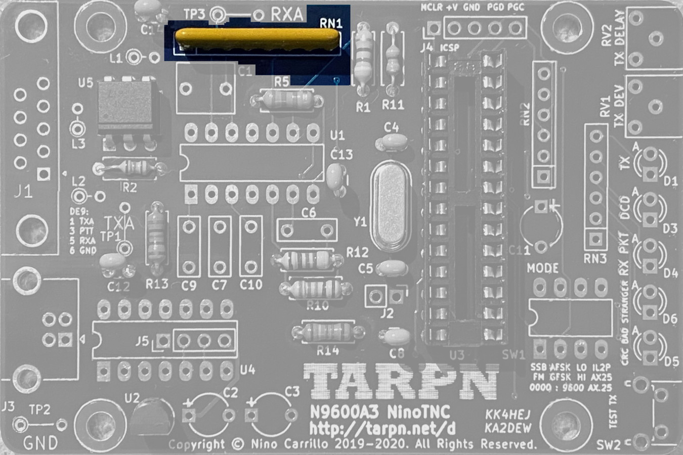
 |
| 17 | RN2 | 5 resistor 47 kΩ resistor network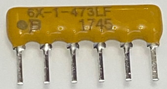
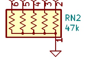 |
Orientation is important!
Pin 1 is identified by the square around the hole on the PCB and an interesting symbol near the end pin on the component. See the prior RN1 step. See schematic symbol below. This provides pull-ups for chip ID and the dip-switch 
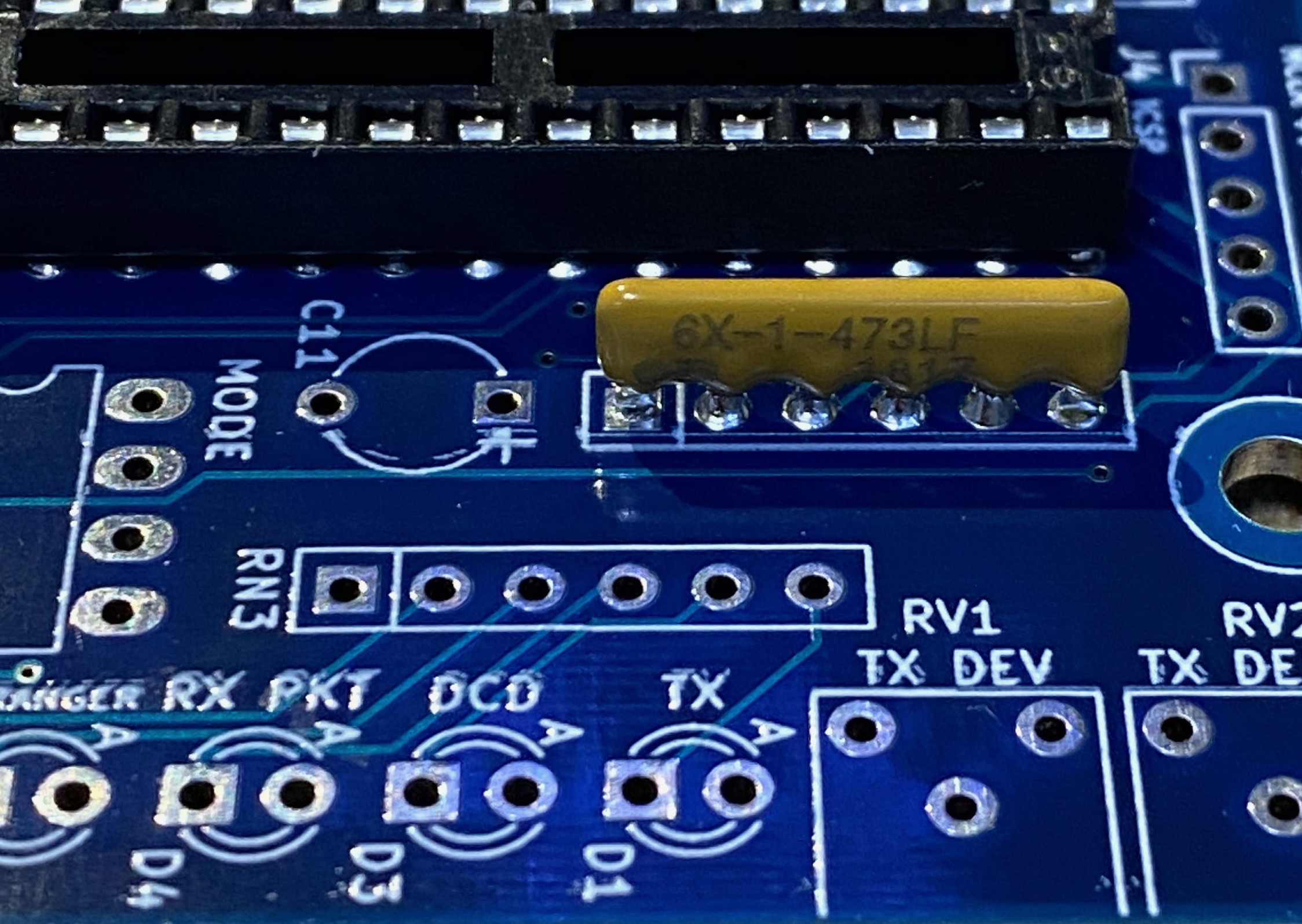 |
| 18 | RN3 | 5 resistor 180 Ω resistor network
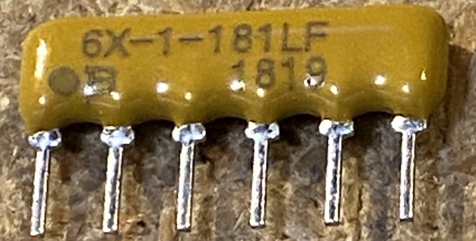
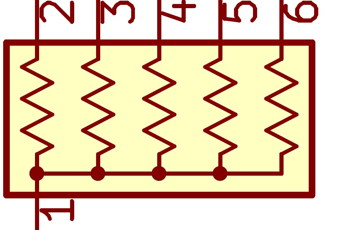 |
Orientation is important!
Pin 1 is identified by the square around the hole on the PCB and an interesting symbol near the end pin on the component. See the prior RN1 step. See schematic symbol below. This provides an in circuit resistance to limit the LED current for 5 LEDs 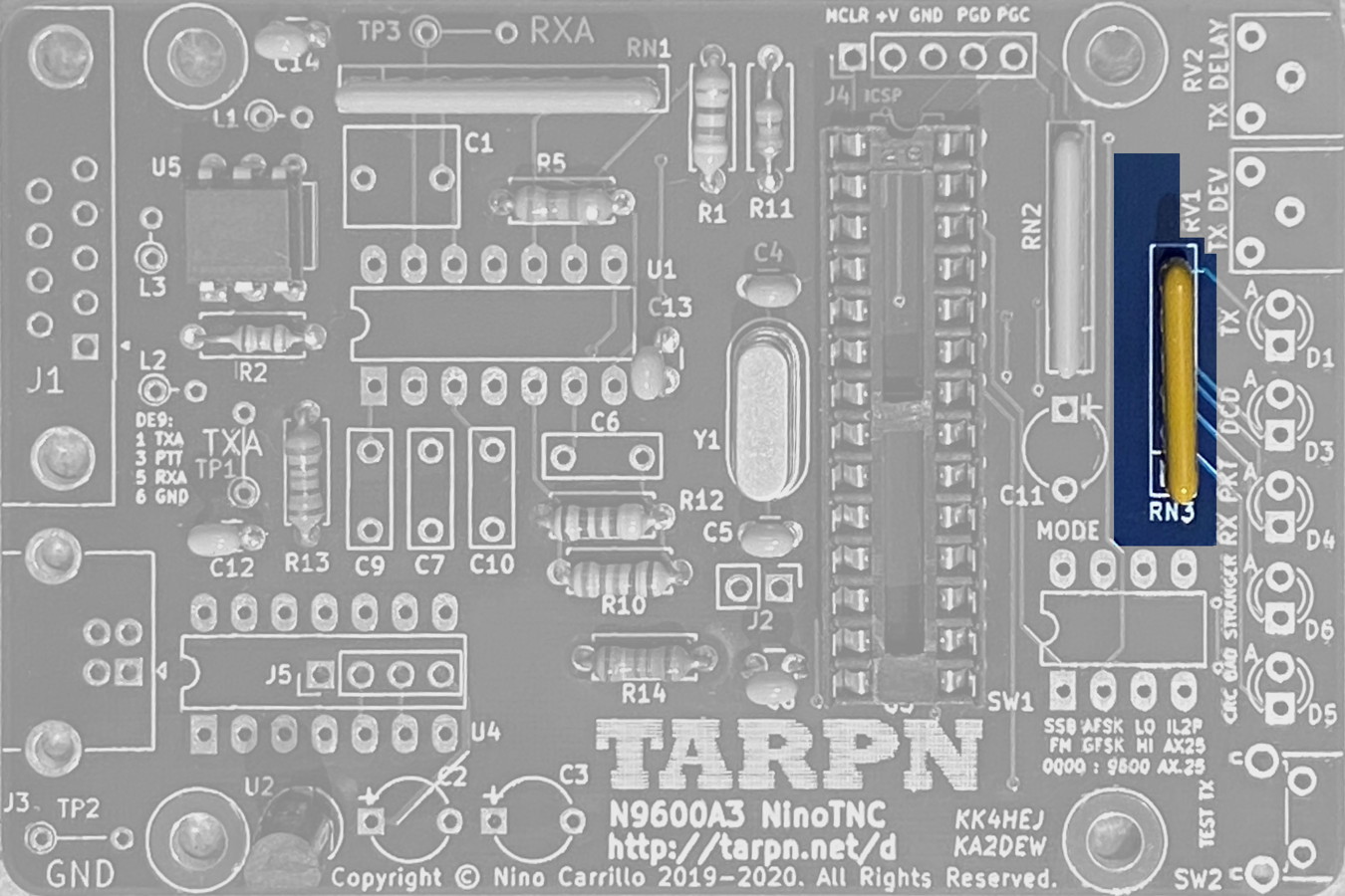
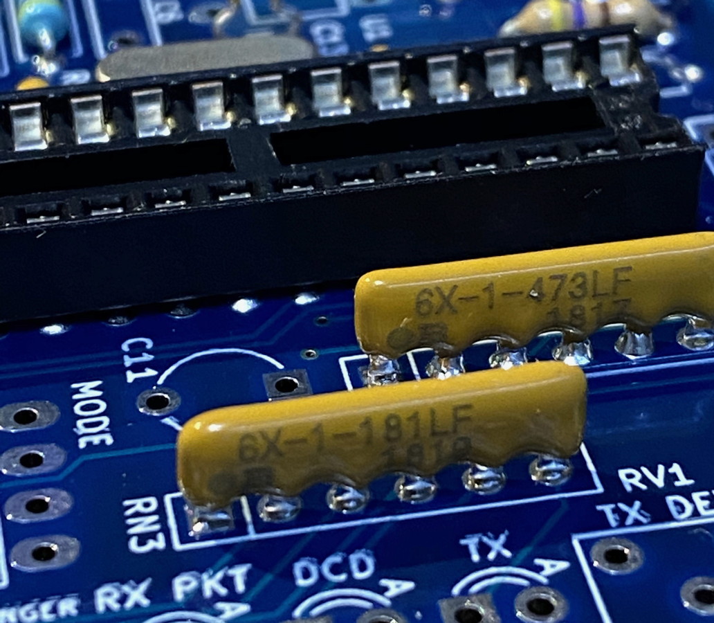 |
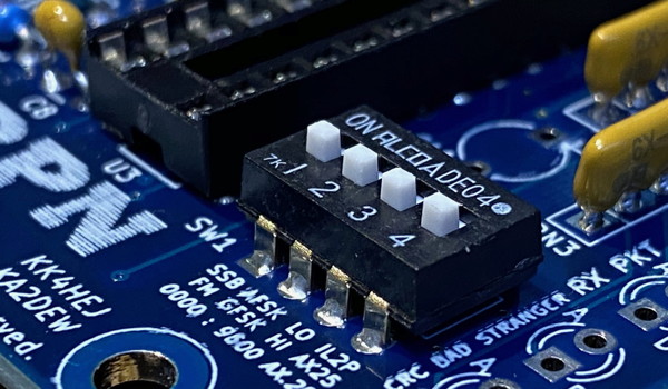
| 19 | SW1 | 4 position dip-switch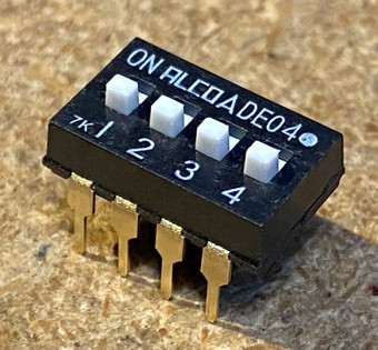 |
Install the switch so the label 1 2 3 4 is toward the TARPN label side of the board.
Each switch is a separate circuit. These switches, and the 47K pull-down resistors in resistor package RN2, drive four separate inputs on the CPU to select options. If the switch is closed (toward the resistor packages), the switch puts VCC into the CPU's GPIO input. If the switch is open (toward the TARPN logo), the resistor pack RN2 resistors pull the GPIO to ground. 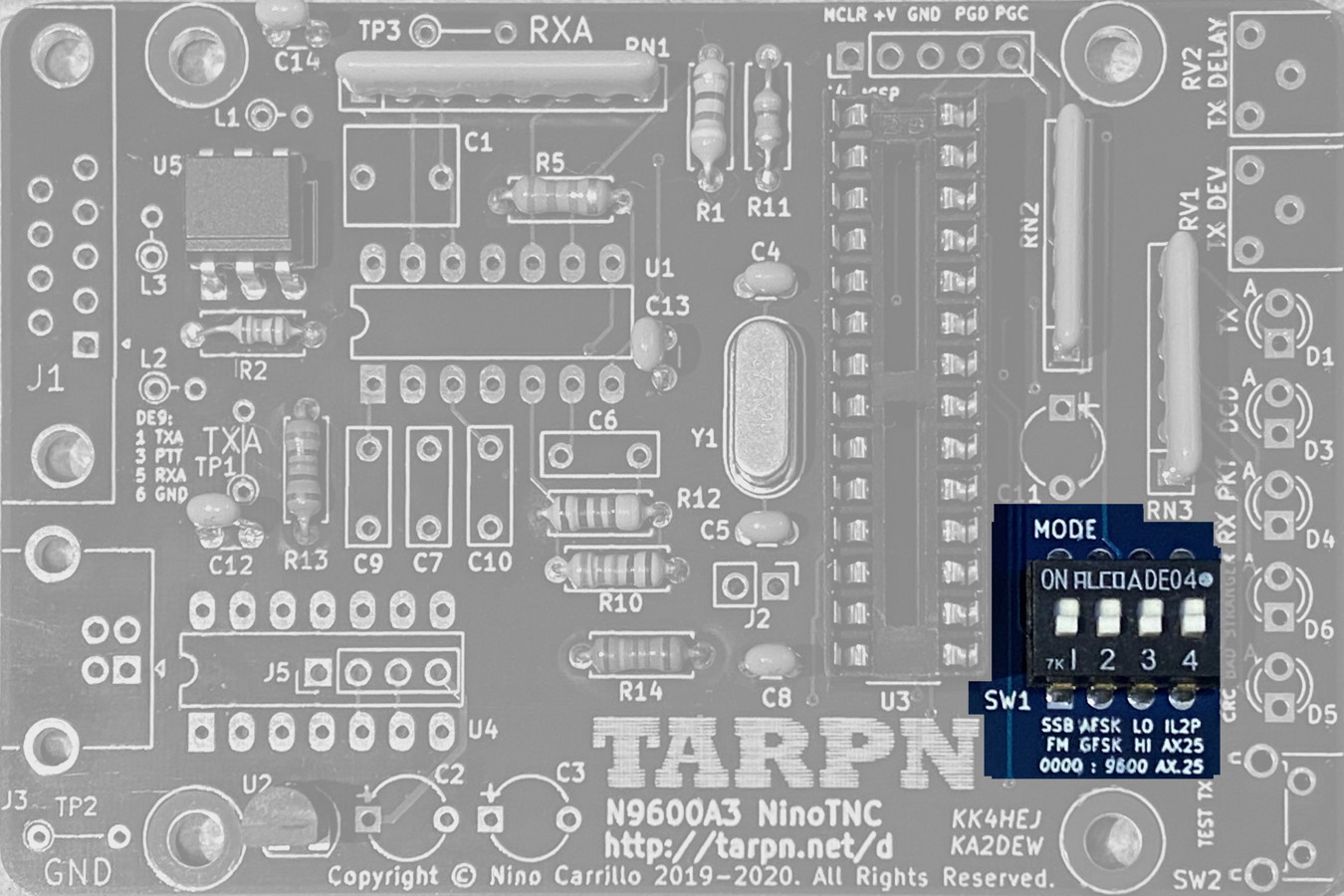
|
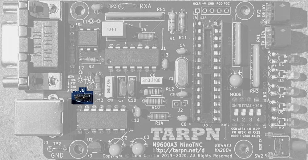
This step is new for the June shipment of A3 boards.
I originally put this step in as a last step but it turned out to be nearly impossible to solder this part in after all of the really tall parts were already installed.
So.. I renumbered all of the steps after step 20. I hope this doesn't cause unrest.
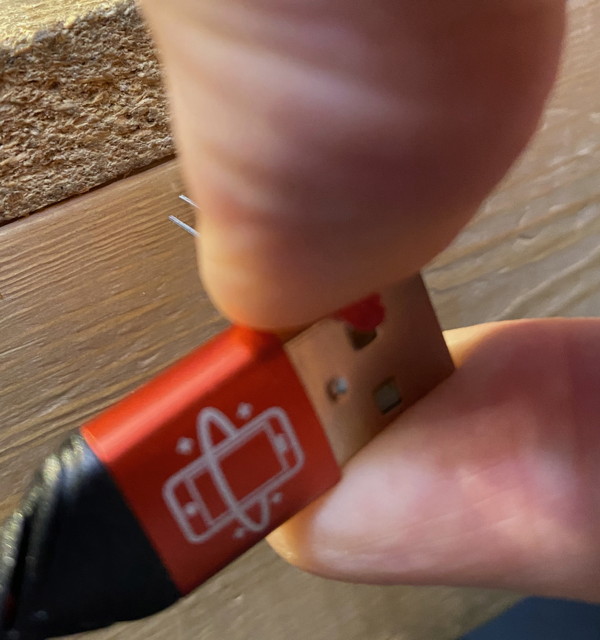
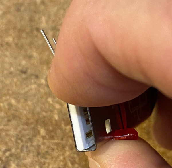
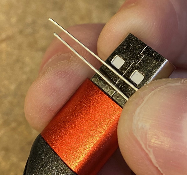
| 20 | J6 | 2 pin jumper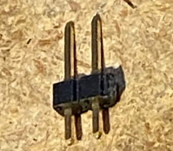
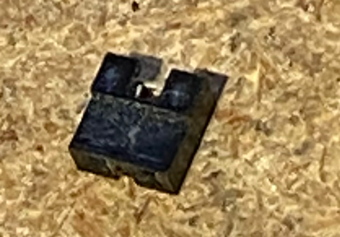 |
This jumper bypasses R3 on the output of the tranmit audio circuit.
In your kit is a plastic widget (called a 'shunt') which covers and shorts out this jumper position.
See picture.
Note that the J6 shunt could be white, red, blue or black.
 |
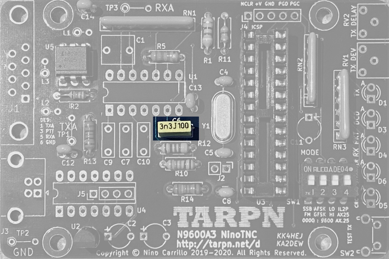
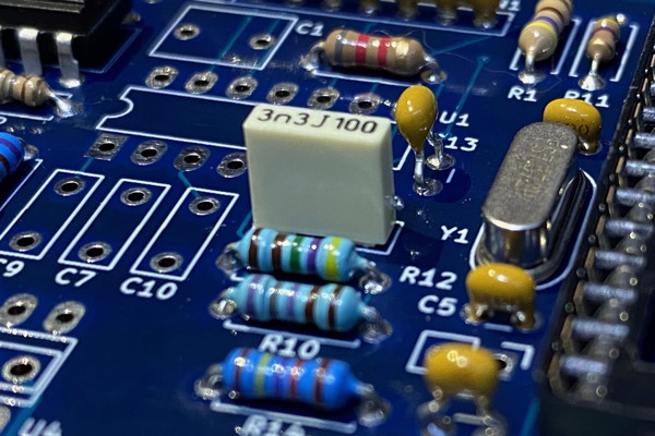
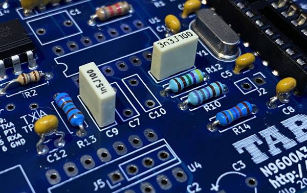
| 21 | C6 | 3300 pF [metal] film capacitor radial leads  |
This is part of the feedback loop in the 2nd stage of the transmit data output.
|
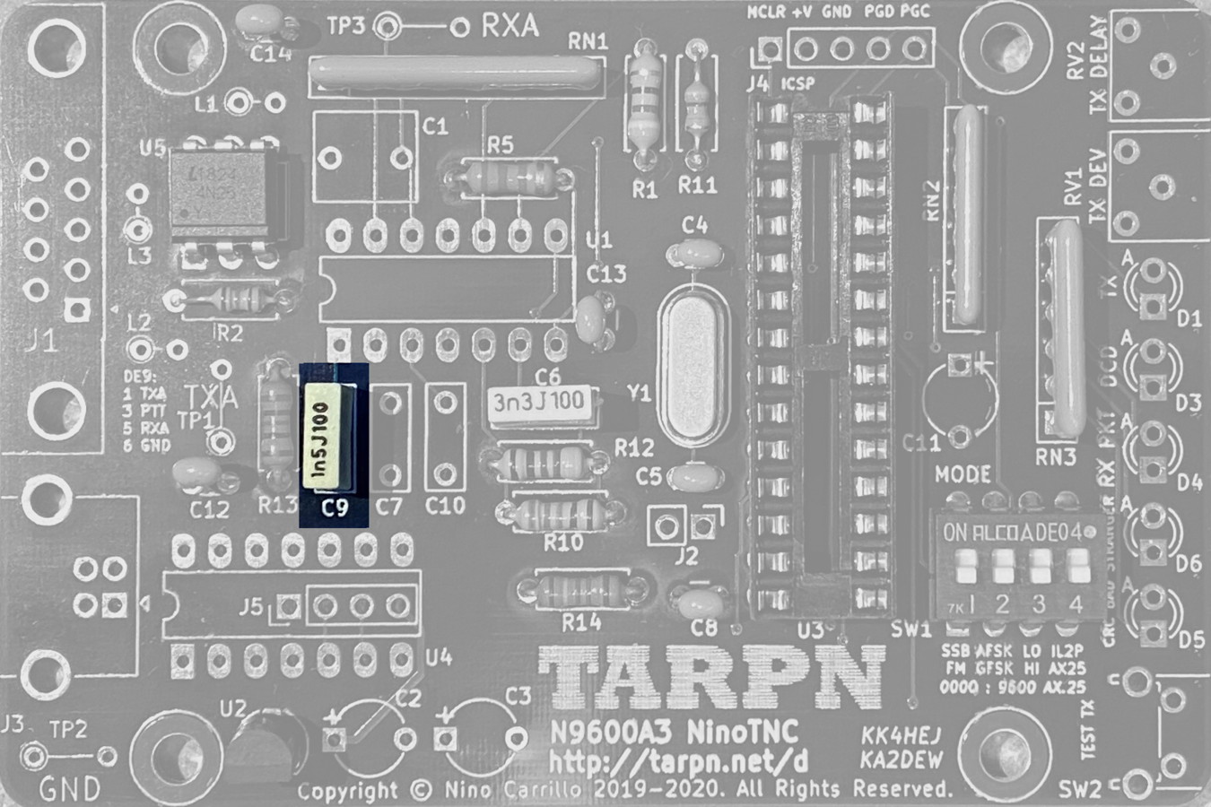
| 22 | C9 | 1500 pF [metal] film capacitor radial leads 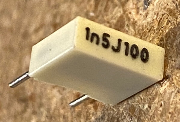 |
This is part of the feedback loop in the 1st stage of the transmit data output.
 |
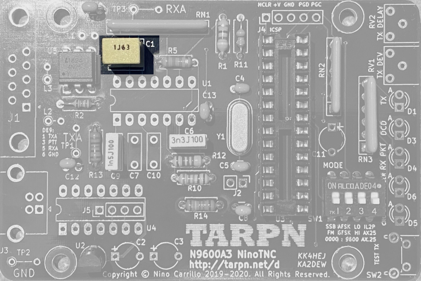
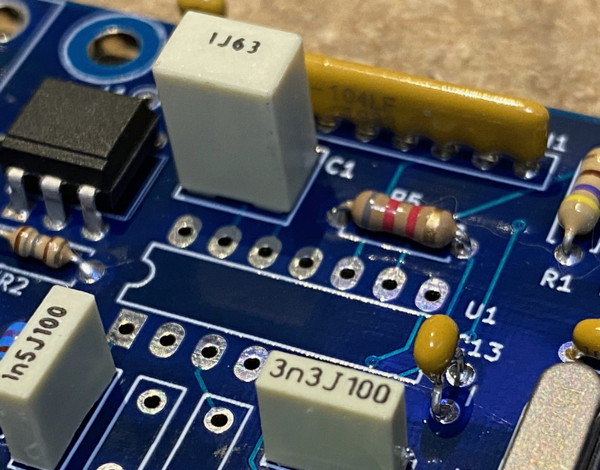
| 23 | C1 | 1 µF [metal] film capacitor radial leads 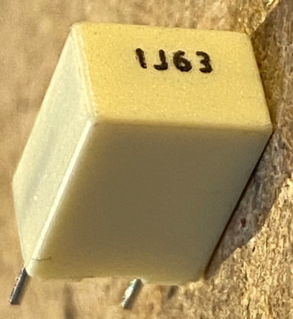
or 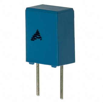
|
This is the capacitive coupling immediately following the DE9 receive data input, before the op-amp receive buffer.
 |
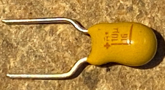
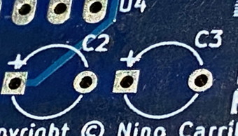
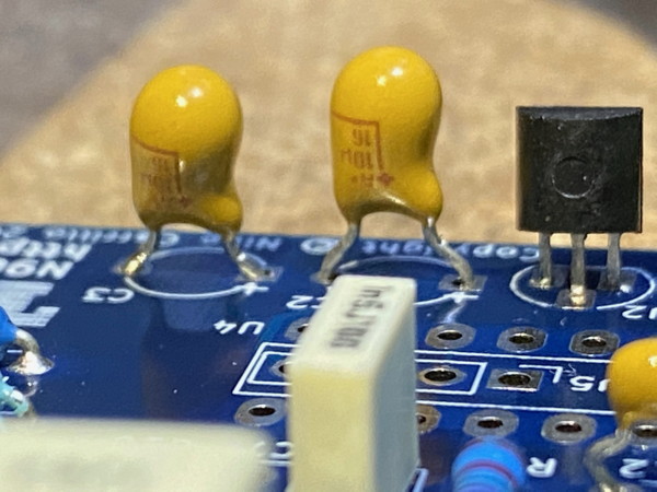
| 24 | C2, C3, C11 | 10 µF 10% 16 V tantalum dipped capacitor 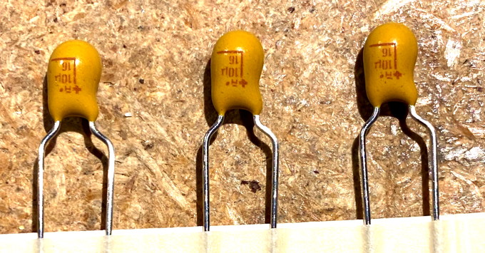
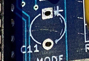 |
Carefully observe values and polarities.
Positive side is marked with a very small plus sign on the part, or a red stripe, and goes into the square solder pad/hole on the PCB.
The silk-screen actually has a microscopic + sign.
C2 is 5v filter on the input to the regulator. C3 is the 3.3v filter on the output from the regulator. C11 is vcap input to the CPU on one side and ground on the other. 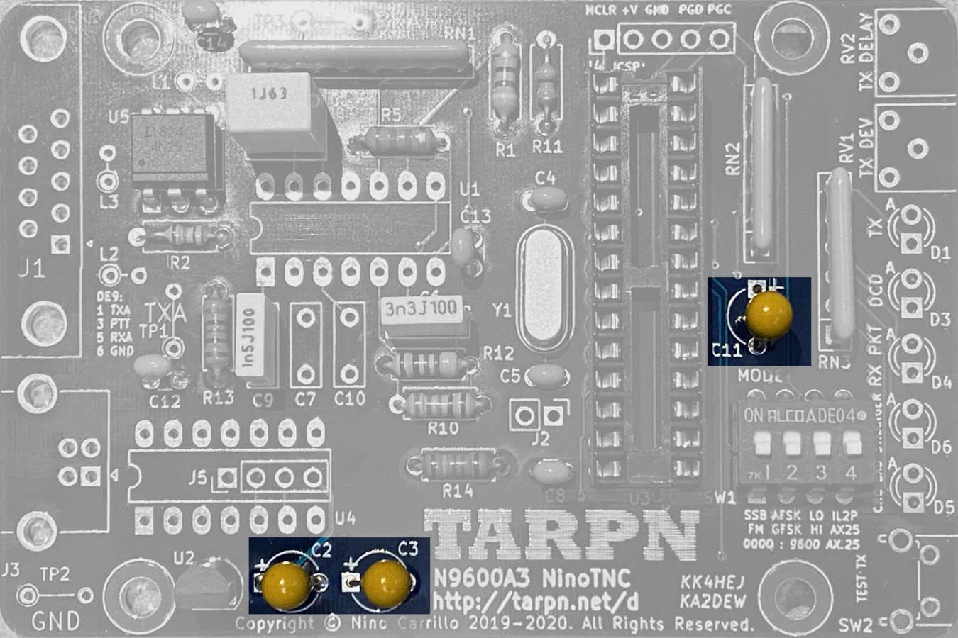
|
| 25 | RV1 | 10 kΩ 1/2 W cermet 1-turn side adjusted trimmer potentiometer. Label="103" 10 * 10**3 = 10000 Ω. 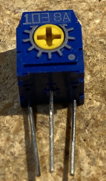
Notice the arrow on one of the legs of the yellow cross. It is pointing down in this image. |
Place in holes so screwdriver adjustable part faces the edge of the board.
This adjusts the Tx Audio level 
|
| 26 | RV2 | 10 kΩ or 100 kΩ 1/2 W cermet 1-turn side adjusted trimmer potentiometer. Label="104" 10 * 10**4 = 100000 Ω or "103" 10 * 10**3 = 10000 Ω. 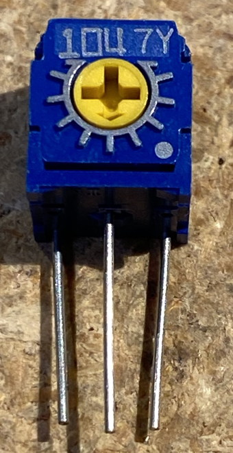
Notice the arrow on one of the legs of the yellow cross. It is pointing down in this image. |
Place in holes so screwdriver adjustable part faces the edge of the board.
This unit adjusts the TXDELAY. The potentiometer selects a voltage between ground and 3.3 V which is passed to an Analog-to-Digital converter pin on the CPU. The resistance of the potentiometer is less important than that the pointer selects a voltage between 0 and 3.3v. A higher value potentiometer would have less leakage between the 3.3 V power supply through the part to ground. But even a 10 kΩ pot only has .33 Milliamps of flow. The potentiometer is read by an AtoD port on the CPU which figures out how much delay between PTT and starting the packet based on the AtoD reading it gets. 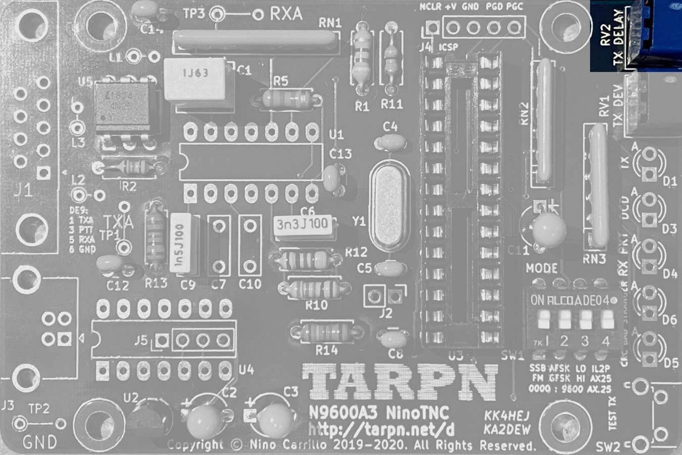 < <
 |
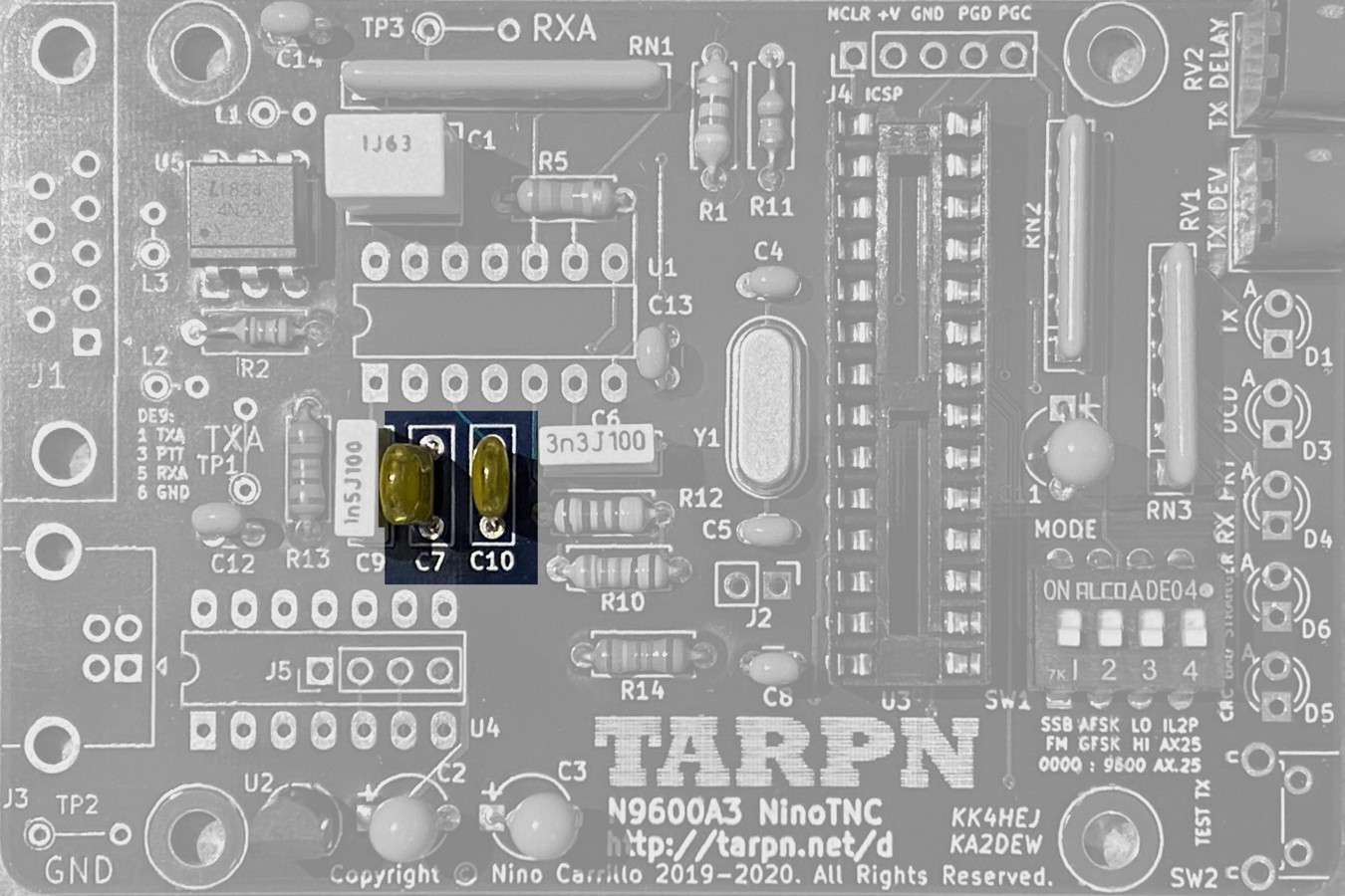
| 27 | C7, C10 | 1200 pF 50v capacitor
light-yellow polyester-film or blue ceramic 
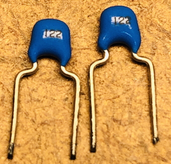
|
In the transmit Op Amp chain, these two capacitors are across the input on each of the first two stages.
 |
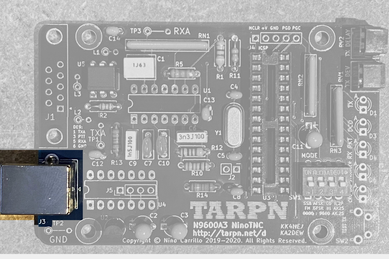
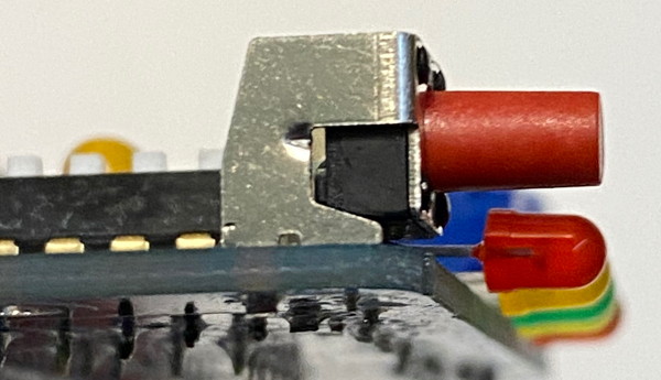
| 28 | J3 | USB-B socket


|
This socket has 6 solder points, two of which look like they'll get in the way when you insert them. They don't.
But they will hold this connector onto the PCB.
Solder all 4 pins and the 2 support items.
 |
| 29 | SW2 | side facing push button switch labelled TEST TX
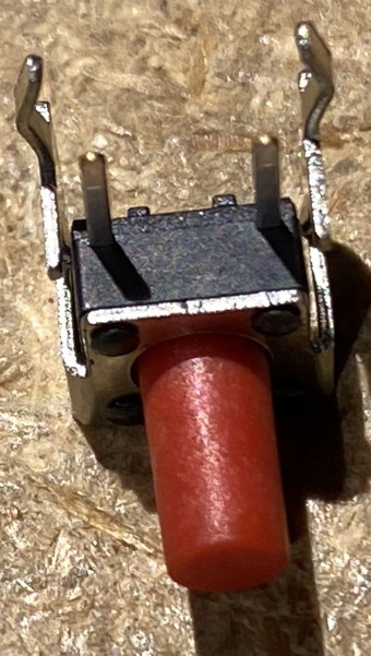 |
Mount so switch button faces off the edge of the board, directly away from the J3-pins in step 24.
Pressing this button connects a GPIO input on the CPU to VCC. Releasing lets the GPIO be pulled to ground through RN2 47 kΩ pull-down resistor. This switch will tell the NinoTNC to transmit a calibrated tone. 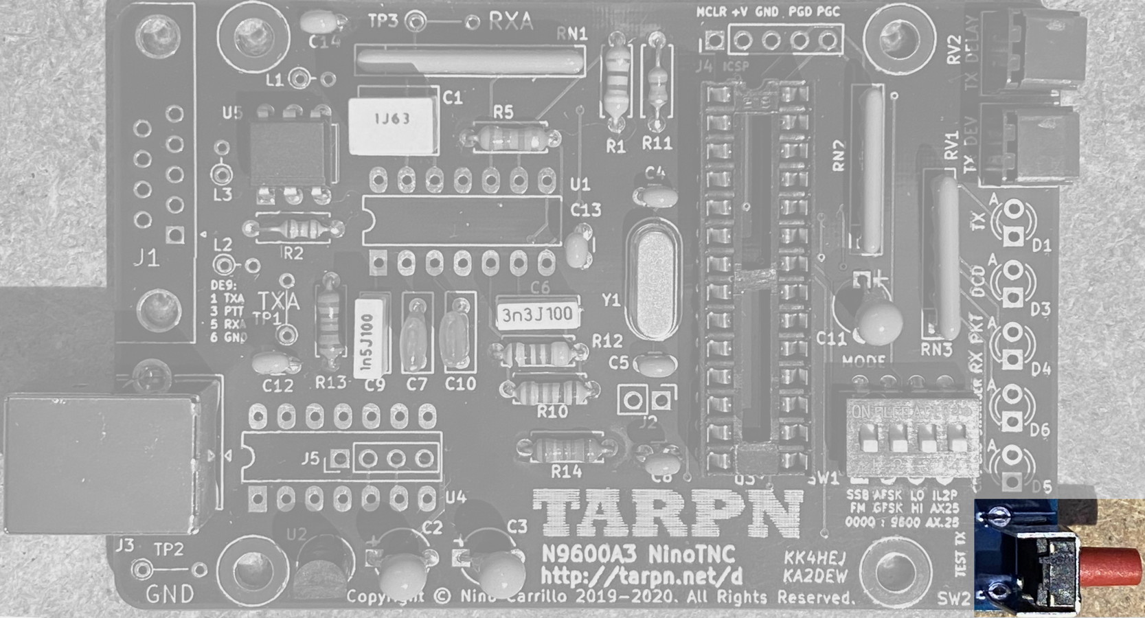
|
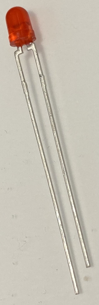
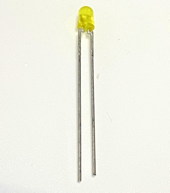
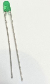
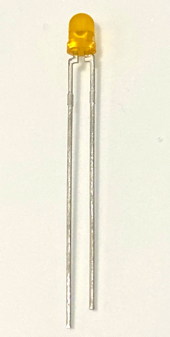
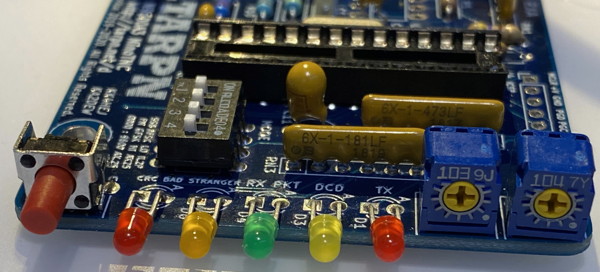
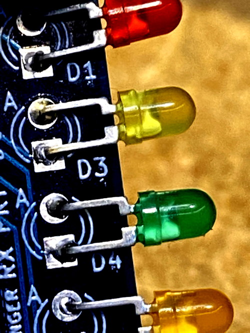
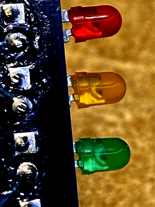
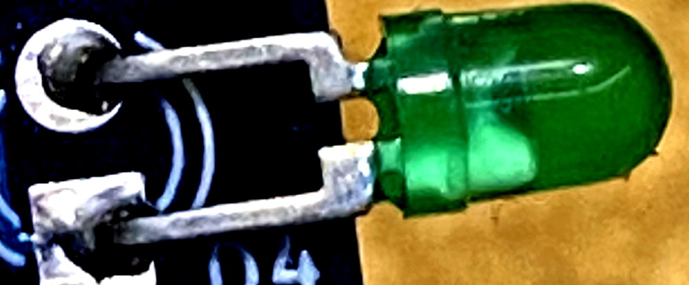
| 30 | D1, D3, D4, D5, D6 | LED installation
|
In this step you are going to bend the leads of all 5 LEDs.
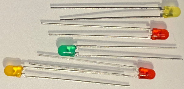
What we need is a fixture to allow all 5 LEDs to be bent the same so they point out the end of the board. It is only critical that the LEDs be perfect lengths and all the same direction if you intend to ever show this NinoTNC to anybody. It's even more critical if you obtain a housing for the NinoTNC made with the LED positions in mind. The leads need to be just long enough before the bend such that the LED lays over the end of the board and just misses the end of the board. We're going to use a USB connector for a guide. It happens to be exactly the correct size. Grab a USB A connector, just like the kind on a keyboard or mouse cable where it plugs into the Raspberry Pi. Put the LED so the short lead is toward the cable side of the connector and the long lead is toward the plug. 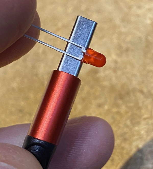
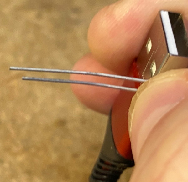
The LED body's base will be against the wide side of the plug and the wires lay around the short side of the plug. 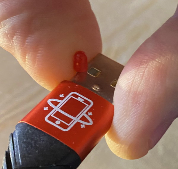
 Now fold the wires over the wide side of the plug making a 90 degree bend.
 Here is the result we want:
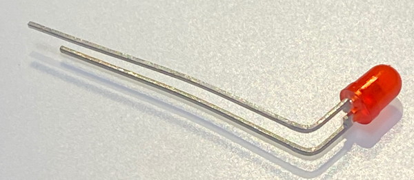
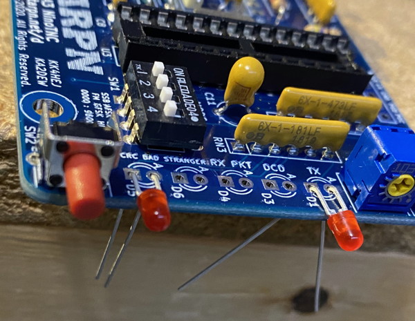 After bending all 5 LEDs, solder them in as shown, then clip and save the trimmings for later use.
|
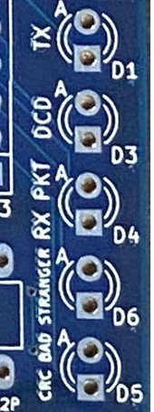 |
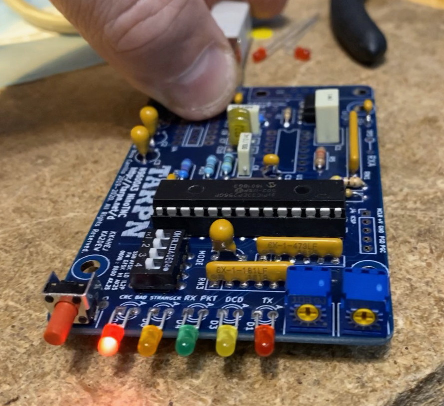
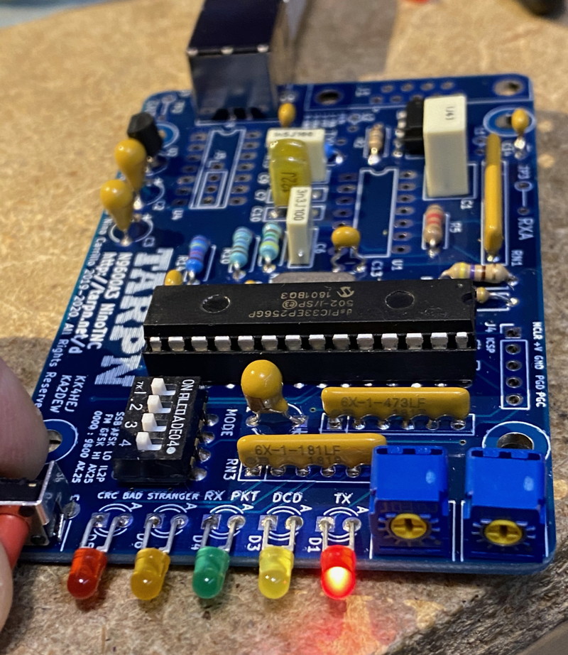
D1 | LED Red diffused
|
TX - This LED is illuminated when the NinoTNC is keying the radio through the opto-isolator. |
| D3 | LED Yellow diffused
|
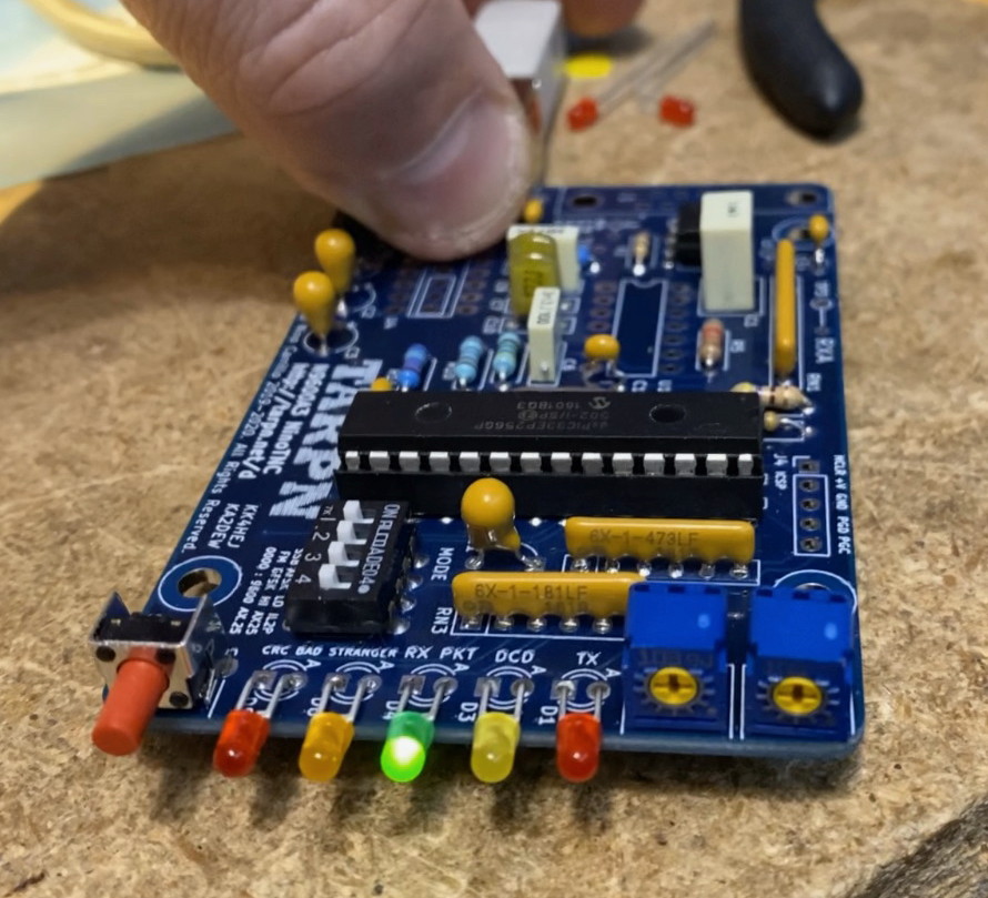
Data Carrier Detect. This LED will illuminate during radio received when several zero crossings occur in the wave-form (noise) which match the selected bit rate. | |
| D4 | LED Green Diffused
|
Last RX packet was decoded properly. This LED remains illuminated until the next receive packet starts, even if the TNC transmits several times before then. | |
| D6 | LED Orange Diffused
|
This LED was the Stranger LED in firmware 2.44 and older. It becomes the Pending LED in firmware 2.45 and newer. This Stranger LED illuminated when a packet is decoded with a sender callsign which does not match any of the callsigns called by this TNC. The Pending LED illuminates when the TNC has a message ready to transmit but hasn't had the opportunity to get rid of it yet. | |
| D5 | LED Red diffused | CRC error on receive packet, This LED illuminates when a valid callsign field is received but the checksum/CRC on the packet doesn't match the rest of the packet and error correction either couldn't be applied, or didn't fix the problem. |
| 31 | U3 | Microchip dsPIC33EP256GP502 CPU
The CPU delivered from ETSY is programmed with released firmware and is ready to be a USB TNC. No reprogramming required for all supported modes. 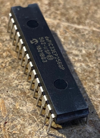 |
To make the chip fit into the socket easily, place the leads on one side against a hard flat surface and push on the package to bend the leads.
Then turn the IC over and do the same thing on the other side.
The pins themselves should be straight, but not splayed out like they are when the IC shipped.
Make sure the half moon on the IC matches the half moon on the socket and on the PCB. 
|

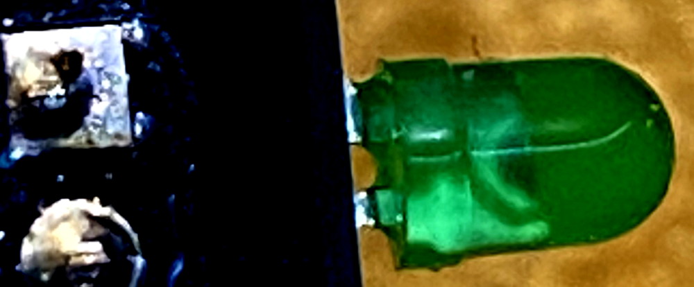
 Closeup of top of back side of PCB with LED. See here that there appears to be a slot between metal pieces inside the bulb.
Now check the photos up above and see if you can tell that the LEDs match on the top photo and on the back photo.
Closeup of top of back side of PCB with LED. See here that there appears to be a slot between metal pieces inside the bulb.
Now check the photos up above and see if you can tell that the LEDs match on the top photo and on the back photo.
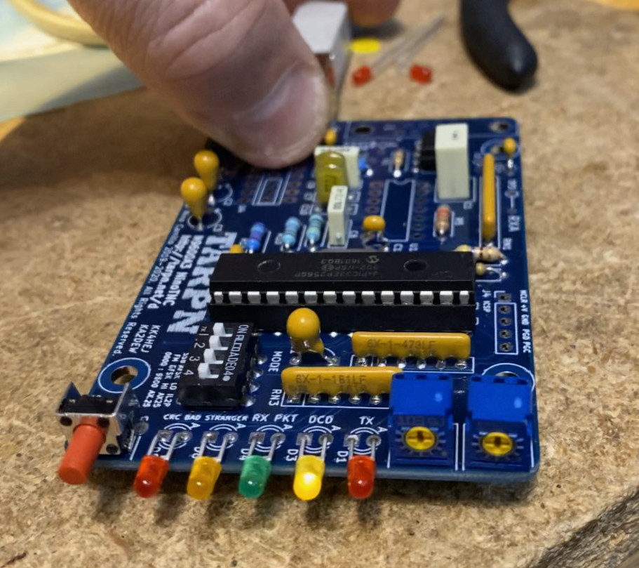
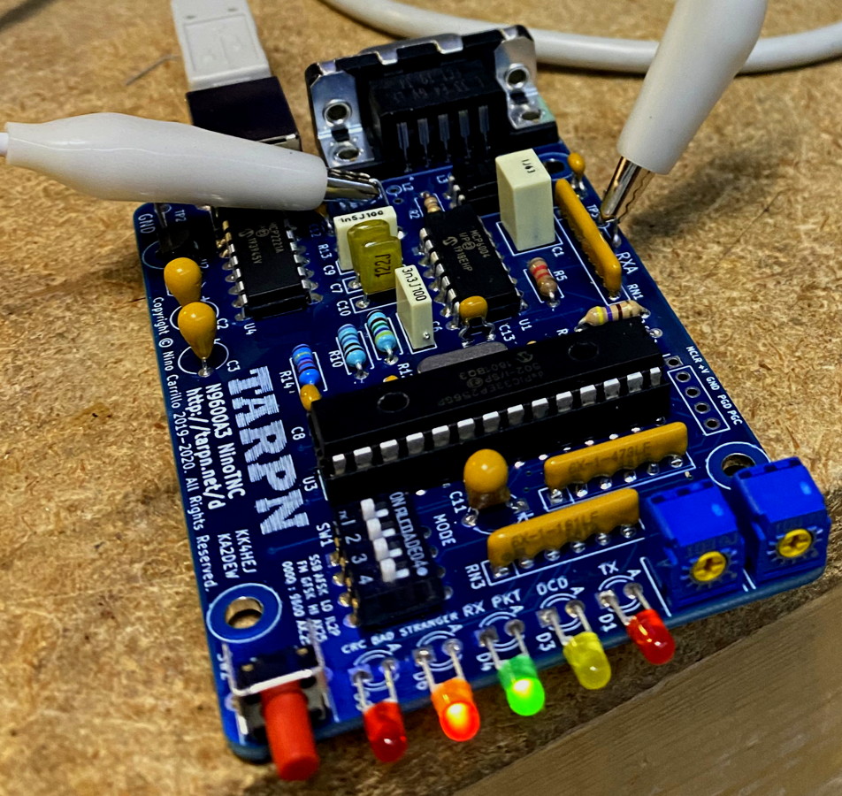
 If your inspection shows the LEDs are installed correctly, reapply power and use your VOM to measure the DC voltage of pins 27 and 28 of the CPU.
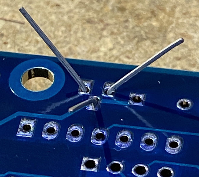
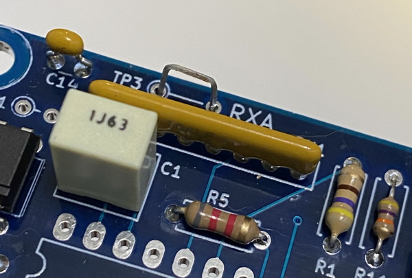
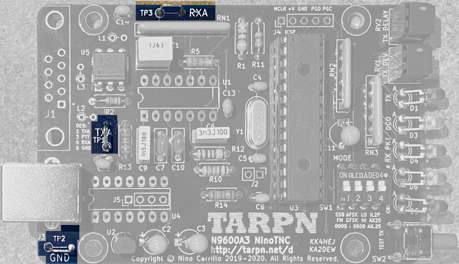
| 32 | Test points TP1, TP2, TP3 | These are loops of scrap wire bent around the blade of a long-nose-plier. 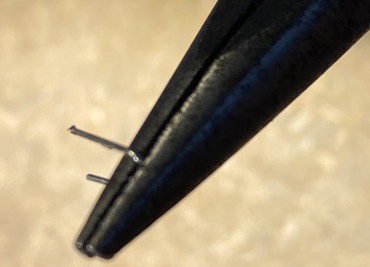 |
Test points for receive audio, transmit audio and ground.
See pix below for installation. 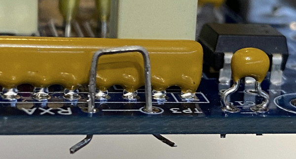
 |
| 33 | U1 | MCP6004 quad op-amp
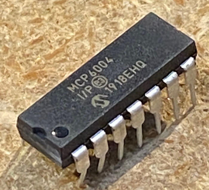 |
Install the MCP6004 quad op-amp Integrated Circuit without a socket.
The pins will have to be bent a little to fit. See step 30.
Since the PCB is now rather crowded, and since the pin bending isn't really obvious,
I recommend test-fitting the IC on the back of the PCB, and then when you get the pins bent as needed, move around to the front of
the PCB and insert the op-amp where it needs to be.
This is a quad-package op-amp (operational amplifier) used to buffer the receive AF data signal from the radio and to condition and buffer the transmit AF data signal to the radio. The quad op-amp has 4 separate amplifier sections. 3 of these are used in the transmit AF signal processing. 1 in the receive. 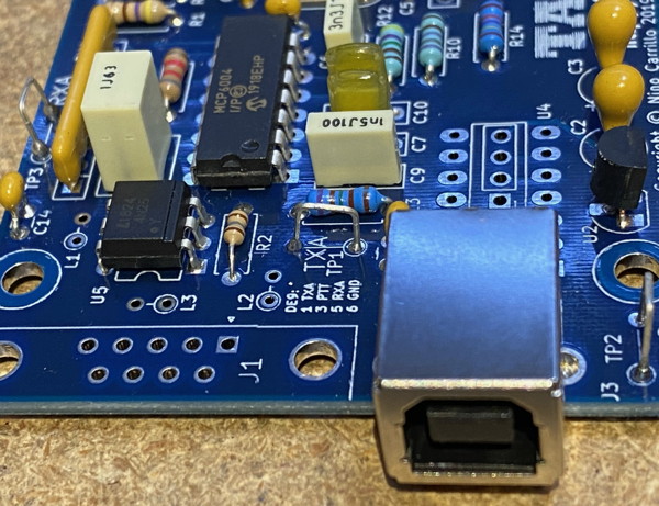
Make sure the half-moon shaped end lines up with the PCB as shown in the photos. 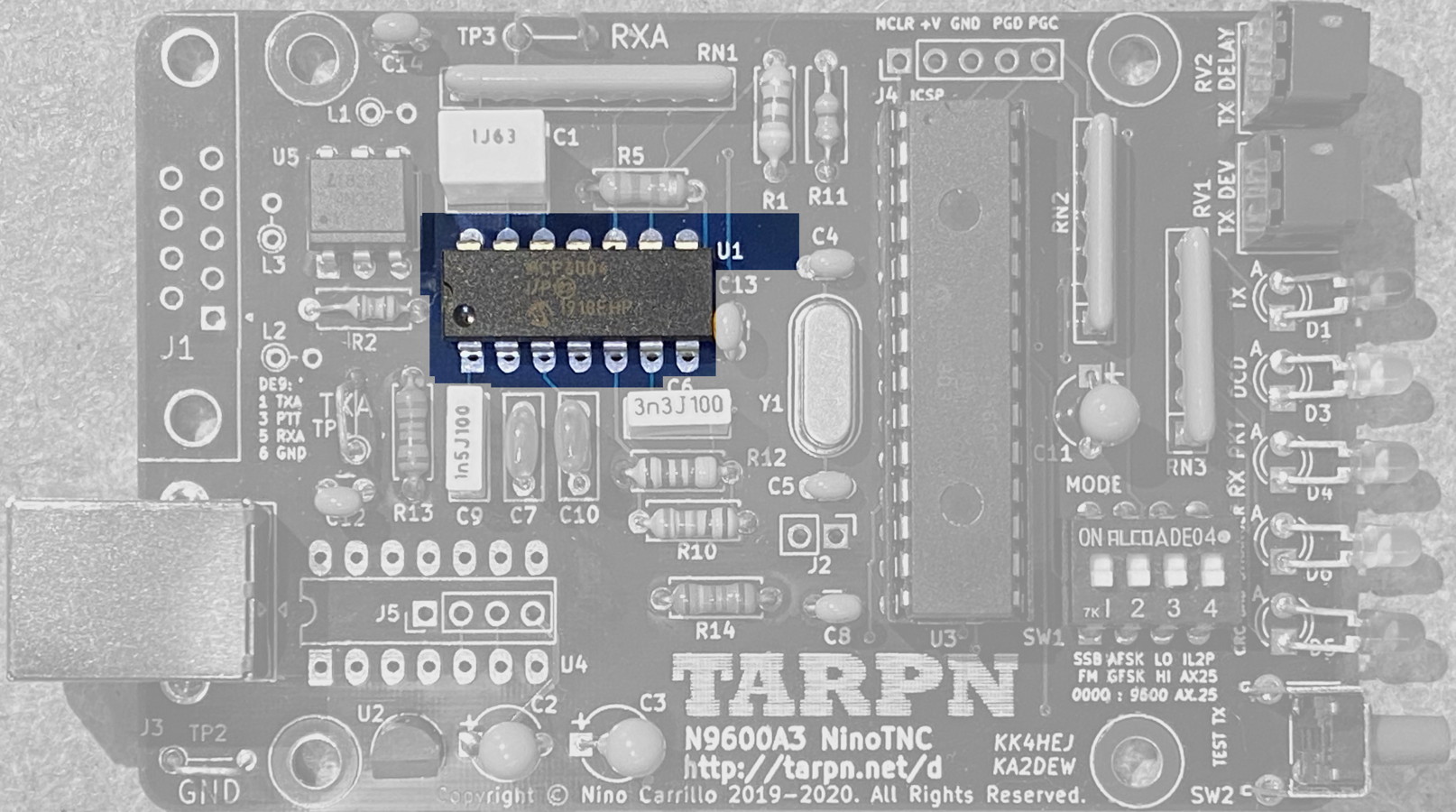 |
| 34 | U4 | MCP2221 or MCP2221A USB interface chip |
Install the MCP2221A USB-serial interface Integrated Circuit without a socket.
Make sure the half-moon shaped end aims toward the USB-B socket. 
Note the extra header pins, J5, underneath where U4 MCP2221 is installed. These pins are for an optional header to be used if the TNC will have a TTL interface and separate 5v source. This could be handy for an embedded project where USB interconnect would be inefficient. If you intend to use a TTL interface to the NinoTNC, don't install U4. 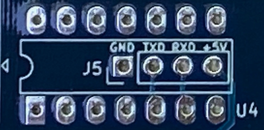
|
| 35 | J1 | DE9 connector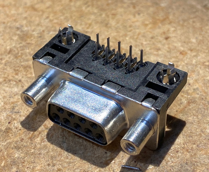 |
This connector is the interface to the transceiver from the NinoTNC.
PTT, TXA data, RXA data, and ground are connected to pins 1, 5, 3 and 6 respectively.
Solder a center pin first, then squeeze the connector into the board and then reheat the center pin. Now solder the remaining 8 pins and then the two outer fingers in 3 places each.  |
| Note | L1, L2, L3 | Ferrite Bead Choke support |
There is room on the board for 3 ferrite beads. The pads for the beads are labelled L1, L2, L3 but they are shorted by a pre-existing trace on the board. Before using one or more of these locations, use a fine-bladed knife to cut the pre-existing trace. Having the ability to install ferrites at these locations would be important if the NinoTNC were seen to reset itself when the connected transmitter is keyed up or if buzzing were present in the transmit audio. |
macmini:tadd$ ls -lrats /dev/*usbmodem*
0 crw-rw-rw-  1 root  wheel   13,   0 Jun 13 10:30 /dev/tty.usbmodem14601
0 crw-rw-rw-  1 root  wheel   13,   1 Jun 13 10:30 /dev/cu.usbmodem14601
macmini:tadd$
pi@raspberrypi:~ $ ls -lrats /dev/ttyACM*
0 crw-rw---- 1 root dialout 166, 0 Jun 13 10:58 /dev/ttyACM0