| home | builders | Search |
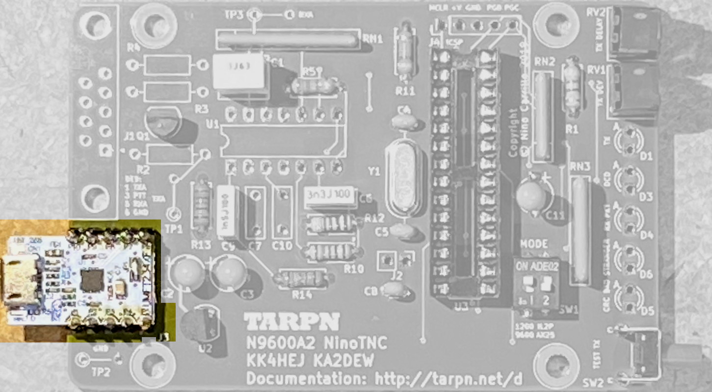
| builders ➜ TARPN Kits and Projects ➜ NinoTNC N9600A ➜ N9600A2 Assembly |
| Bill Of Materials |
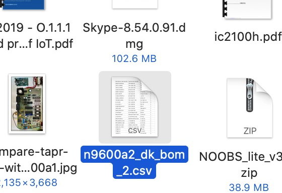
Right-click on this link and save n9600a2_dk_bom_9.csv to your computer.
This is the Digikey shopping list for the TNC. Find the n9600a2_dk_bom_4.csv file on your computer. |
|
| Go to Digikey website | Click on this link: Digikey |
|
| Shopping Cart | Click on the shopping cart. If presented, click on View Cart button. |

|
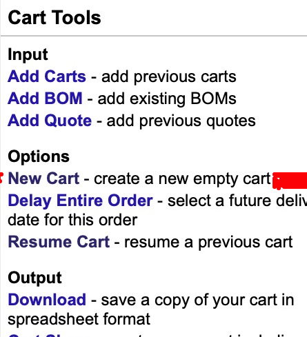
| New Cart |
if there is no New Cart button, skip to Upload CSV, else click the New Cart button. |
|
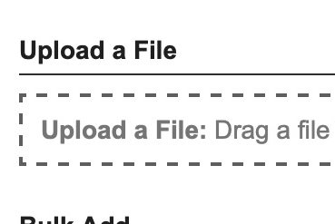
| Upload CSV |
There is an Upload A File field in the middle of the form.
Drag the CSV file from your Finder/Explorer into that field, or click on the Browse link, and then navigate to the CSV file. |
|
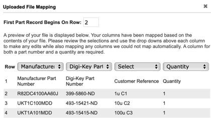
| Confirm Mapping |
You will see a pop-up window titled "Upload File Mapping".
Find the titles (in row 1) on that window and make sure the column headers match the text in the title row. Make sure the third column ROW drop-down says "Customer Reference". Click on Add To New Cart |
|
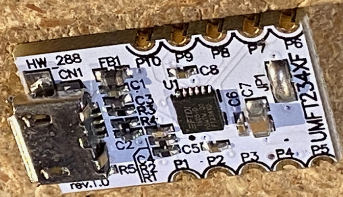
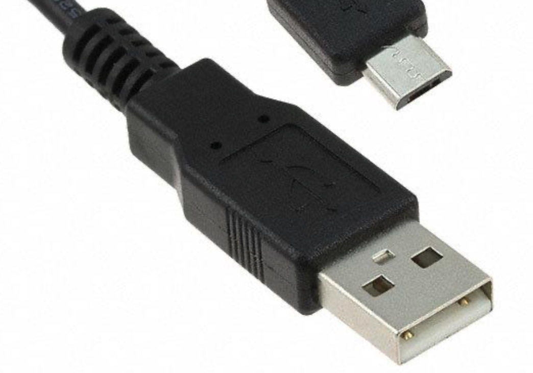
| USB cable? |
If you need a USB A male to micro USB B male cable, add it now. Search using All Products search box on Digikey page.
Part# Q968-ND is $2.67 for a one-foot cable or Part# 380-1431-ND is $2.01 for a 3'4" cable. Short is better for RF immunity. |
|
| Checkout |
Now do checkout and pay for your order.
USPS shipping is the cheapest. Paypal works. |

|
| ⇒ All parts are inserted from the silk-screened side of the board, i.e. from the side on which the white writing is printed. |
| ⇒ Except where specifically noted, all two pin components are non-polorized so you can put the part onto the board with the pins in either hole. |
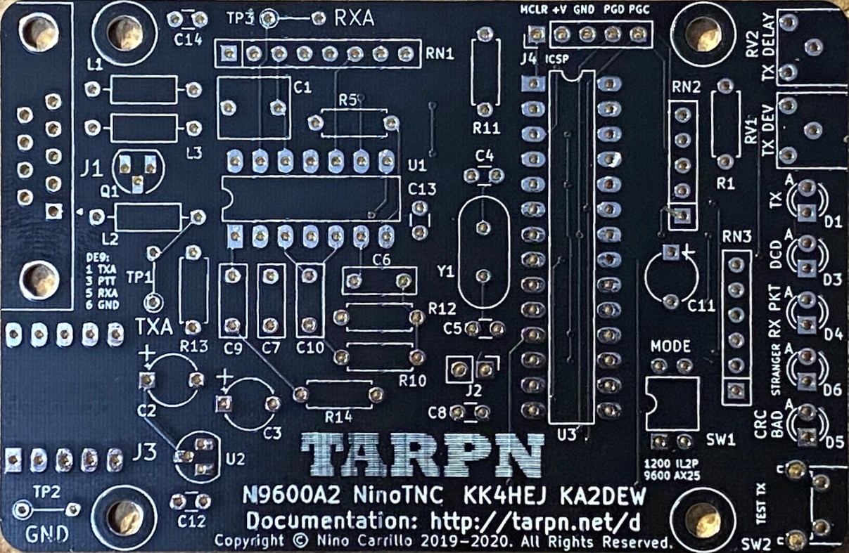
| 1 | Y1 | 7.3728 MHz crystal
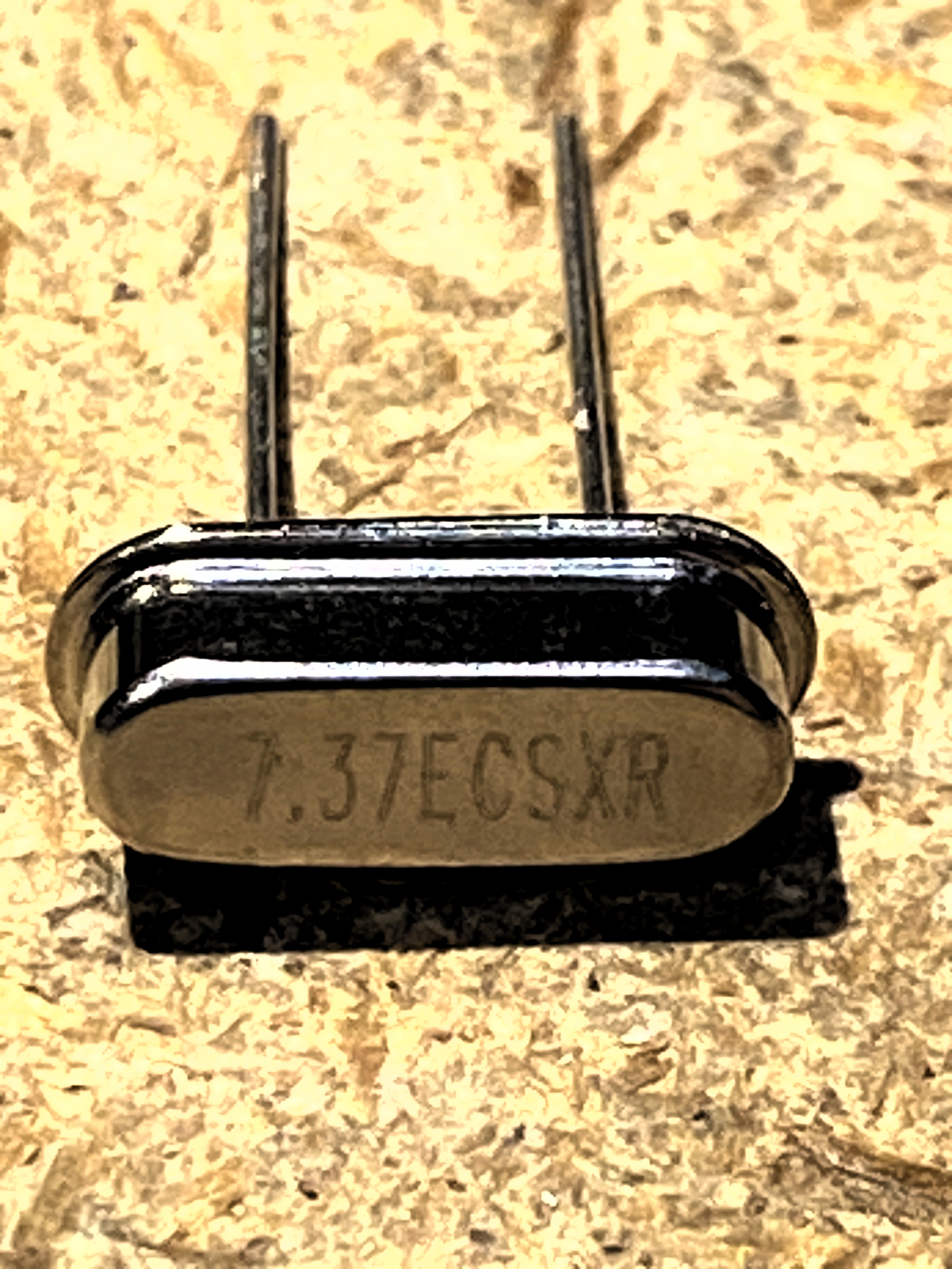 |
The crystal will have some lettering on it containing the numbers 7.37
The crystal and two capacitors forms an oscillator to provide clocking for the CPU's digital circuits. 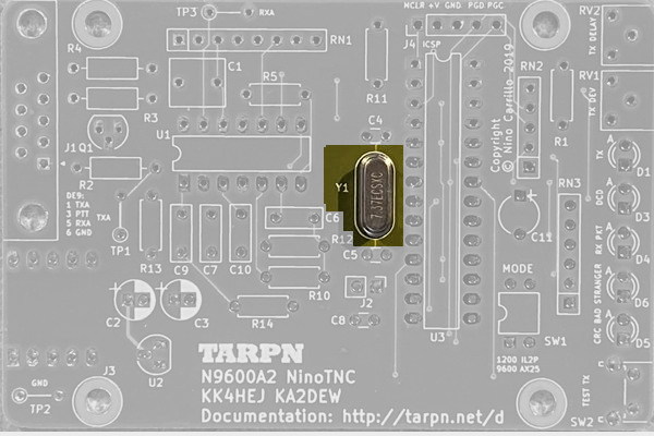 |
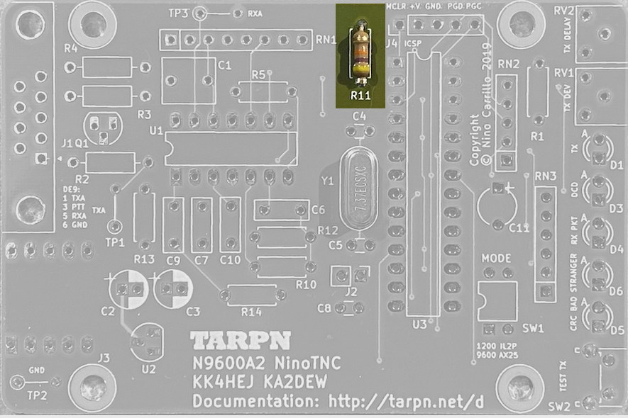
| 2 | R11 | 47K ohm 1/4 watt 5% resistor
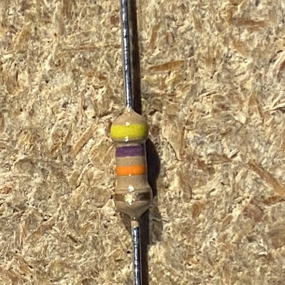 |
R11 turns off the MCLR input to the CPU.
 |
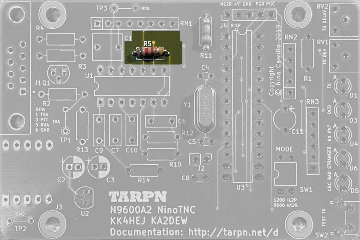
| 3 | R5 | 8.2K ohm 1/4 watt 5% resistor
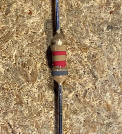 |
In the TX-data/audio path between U1B and U1C op amp devices.
 |
| 4 | R1 | 470 ohm 1/4 watt 5% resistor 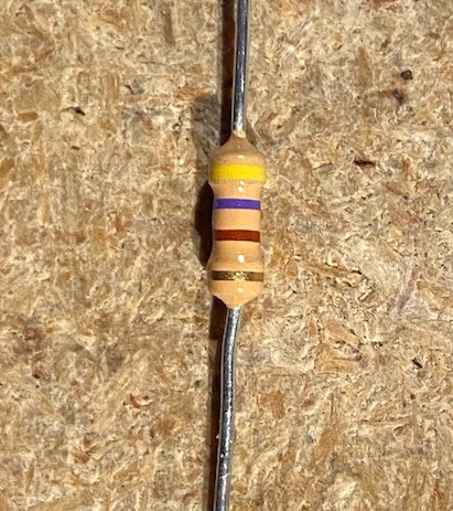 |
This is a low-end-limit to the Deviation adjust. 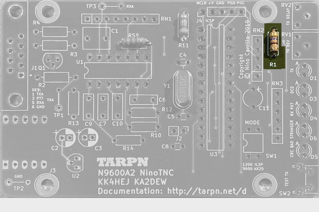 |
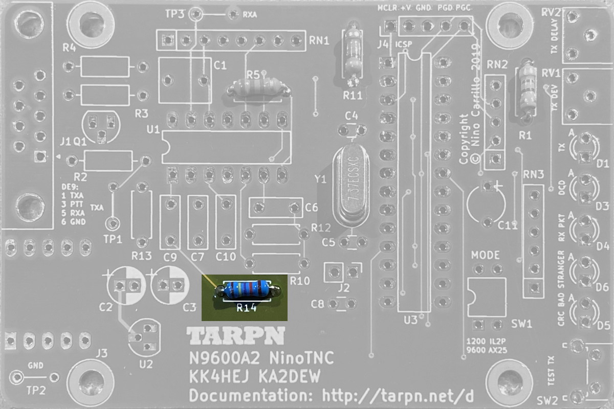
| 5 | R14 | 14.7k ohm 1/4 watt 1% resistor 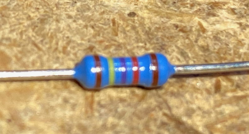 |
This is part of the amplifier circuit for the 1st op-amp stage in the transmit data circuit.
 |
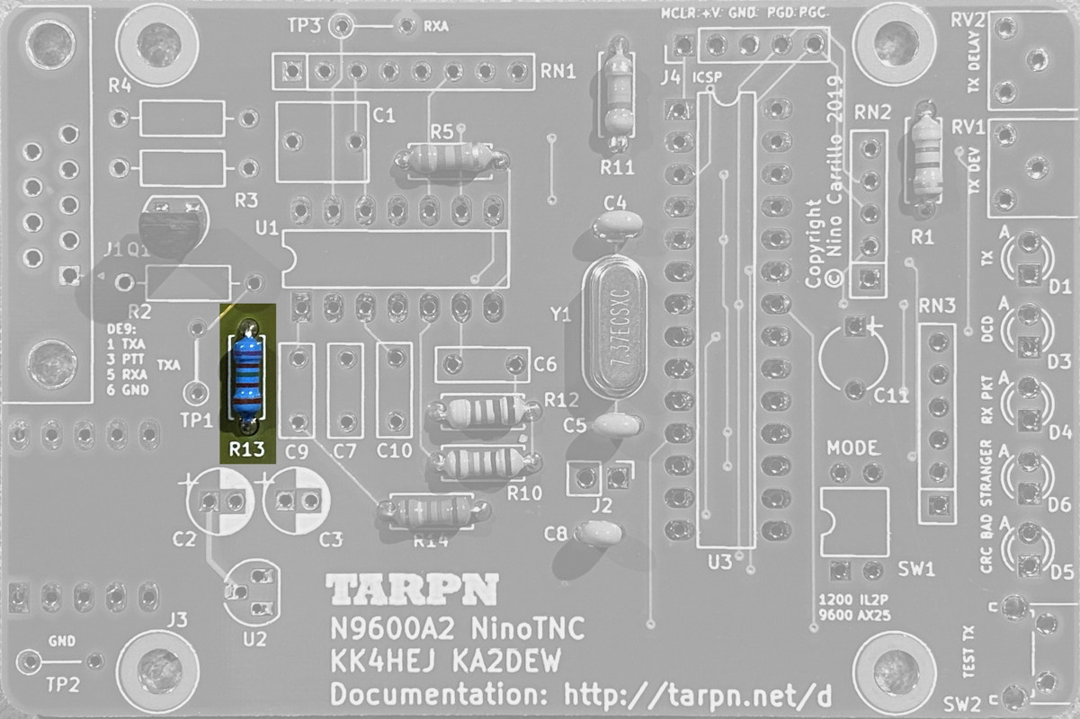
| 6 | R13 | 7.15k ohm 1/4 watt 1% resistor 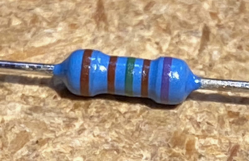 |
This resistor is in the input and feedback loop for the 1st op-amp stage in the TX-data/audio path.
 |
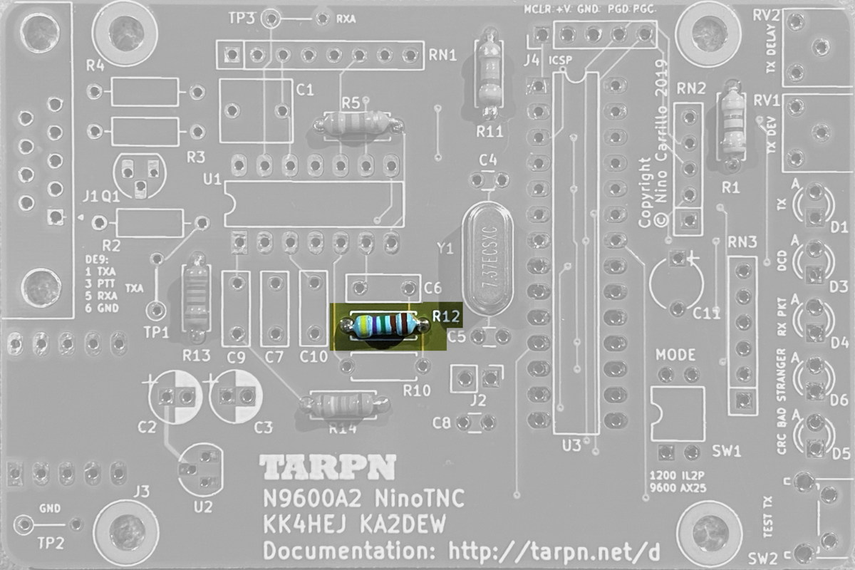
| 7 | R12 | 4.75k ohm 1/4 watt 1% resistor 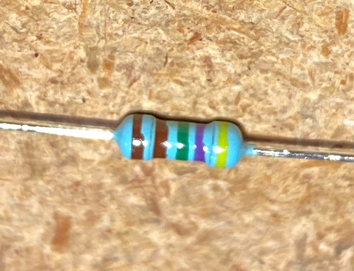 |
This resistor is in the audio path between the 1st and 2nd op-amp stage in the TX-data/audio path.
 |
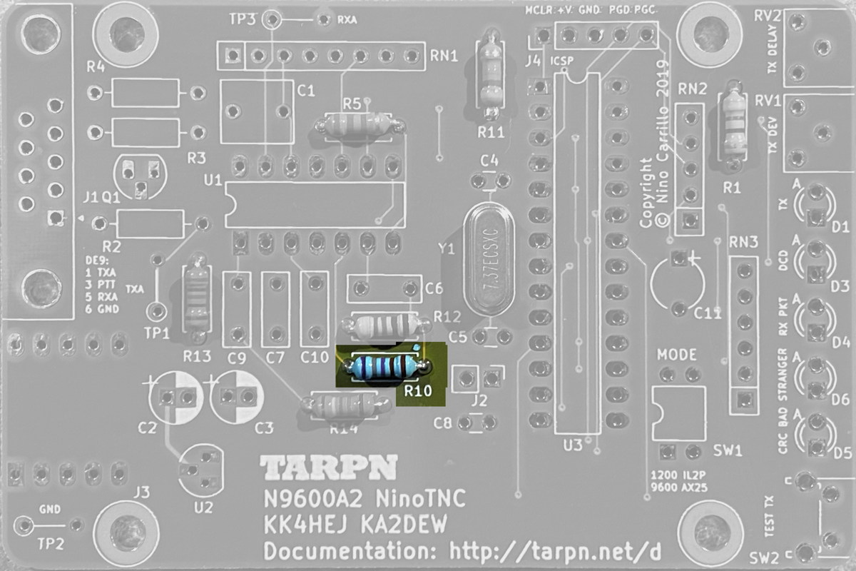
| 8 | R10 | 7.87k ohm 1/4 watt 1% resistor 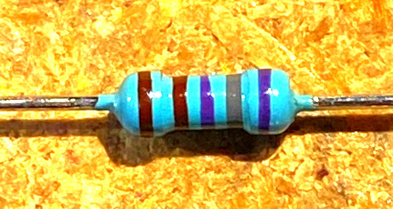 |
This resistor is in the input and feedback loop for the 2nd op-amp stage in the TX-data/audio path.
 |
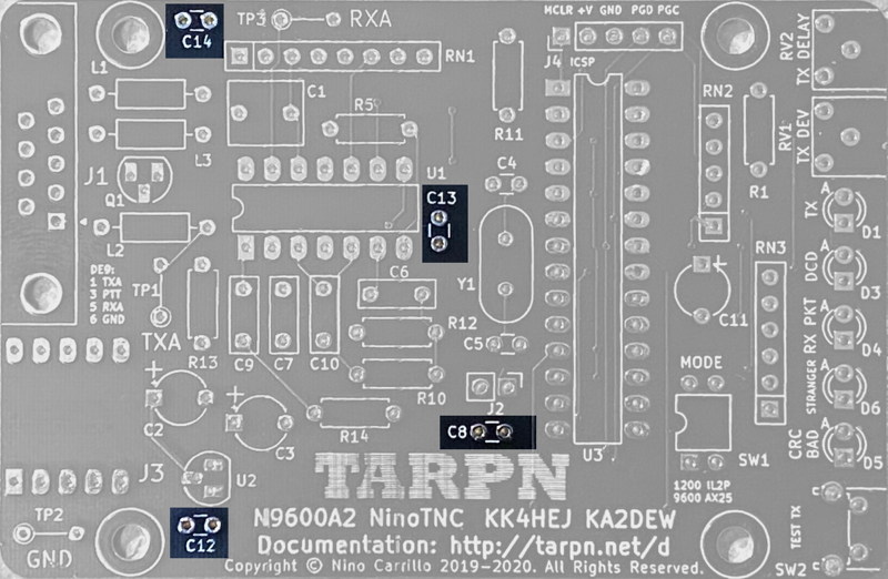
| 9 | C8, C12, C13, C14 | 0.1uF 10% 50v Ceramic capacitor 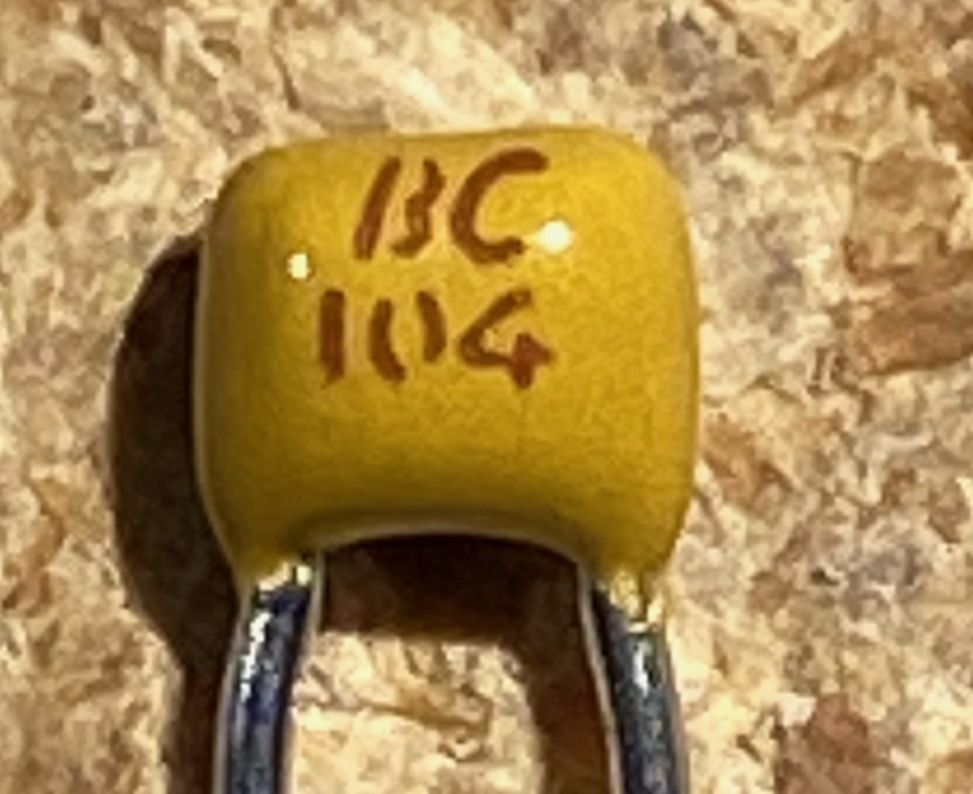 |
These ceramic radial capacitors provide power supply filtering and glitch reduction on the CPU’s main power input and at 3 other places around the board. .
 |
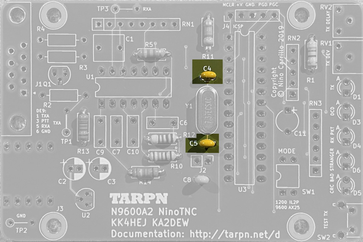
| 10 | C4 and C5 | 18pF 5% 50v Ceramic capacitor 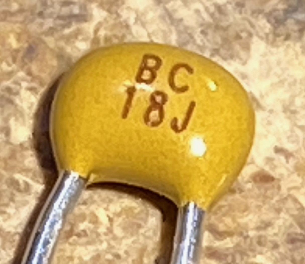 |
C4 and C5 are part of the crystal oscillator circuit
 |
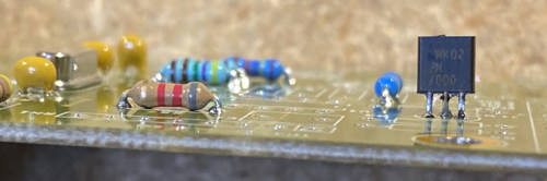
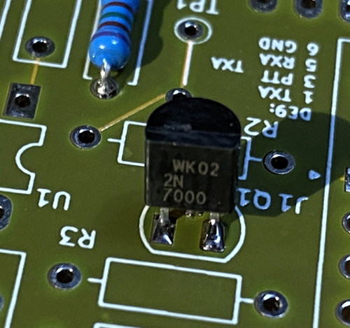
| 11 | Q1 | 2N7000 transistor 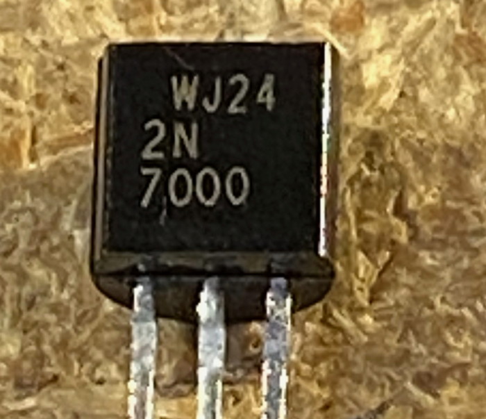 |
Pay attention to the shape of the silkscreen box where this part is inserted.
The flat side of the transistor lines up with the flat side of the silksreen shape.
This transistor is driven by a GPIO on the CPU and is responsible for pulling the PTT line to ground. If this transistor is missing or dead, the TX LED on the TNC will still light, but the radio will not transmit. 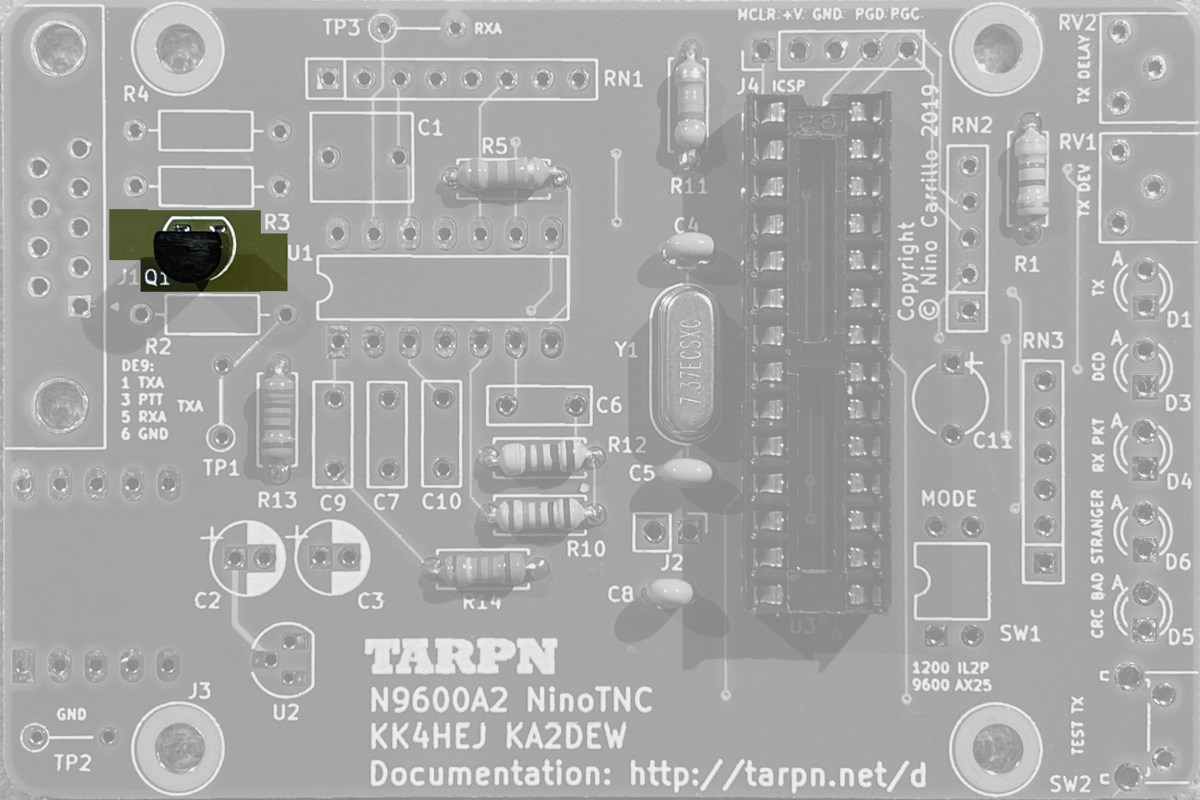 |
 |
|||
 |
|||
| 12 | socket U3 | 28 pin DIP IC socket
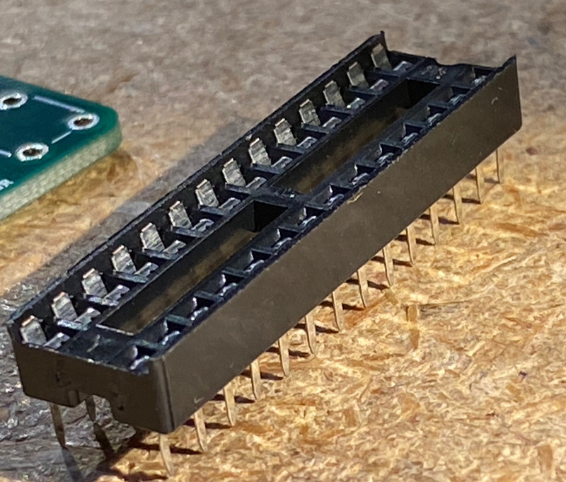

 |
 |
| 13 | U2 | 1702 3.3v 250mS TO92 case regulator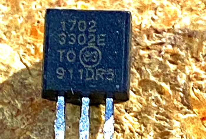 |
This part takes the 5v DC from the USB connector and regulates it down to 3.3v, as needed by the CPU.
Align flat edge with the board silkscreen 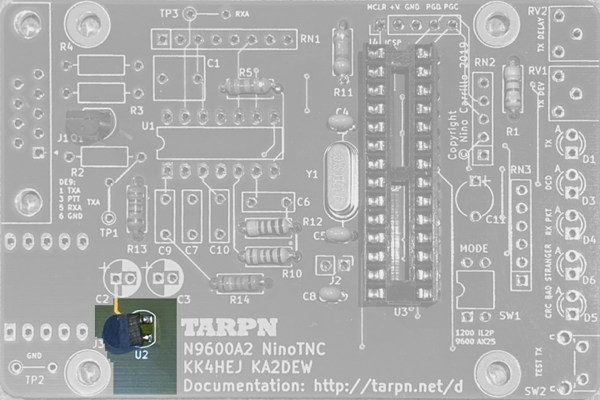 |
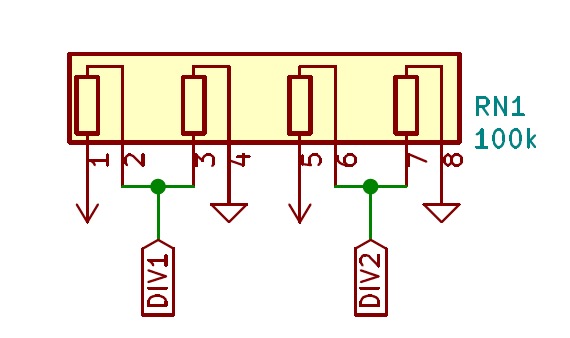
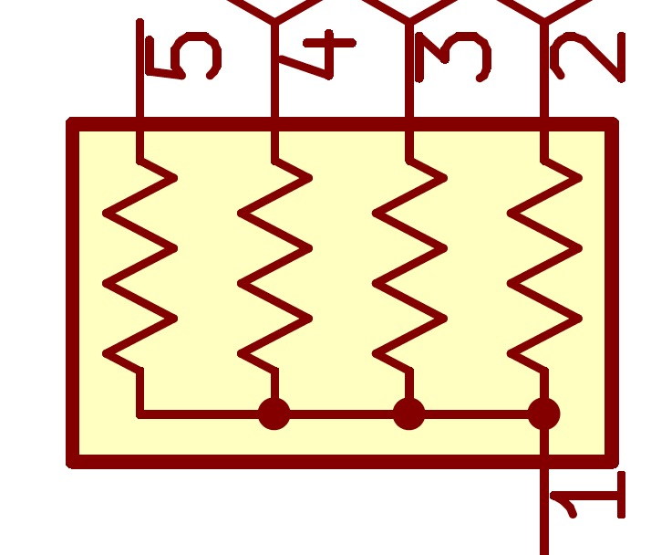
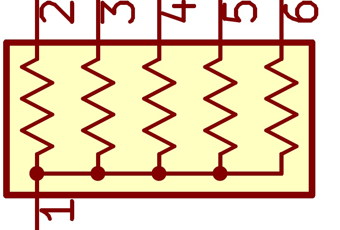
| 14 | RN1 | 4 resistor 100k-ohm resistor network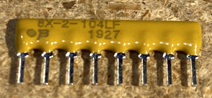 |
Pin 1 is identified by the square around the hole on the PCB and an interesting symbol near the end pin on the component.
See schematic symbol below. If you are looking at the print on the one side of the resistor pack such that the pins are down, then pin1 is on the left.
This part serves as a pair of resistor voltage dividers. The first follows the input audio coupling capacitor so the voltage of the RX audio is centered around 3.3v/2. The second is used to provide a bias to the C element of the MPC6004 quad op-amp package in the final stage of the TX audio shaping. 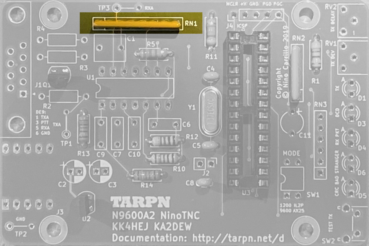 |
 |
|||
| 15 | RN2 | 4 resistor 47k-ohm resistor network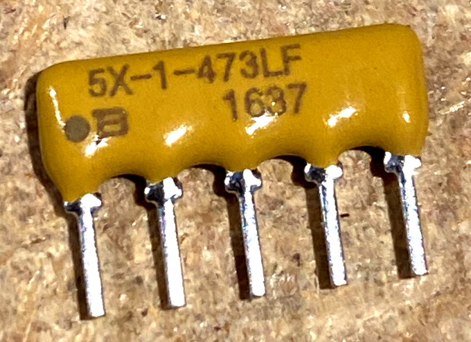 |
Pin 1 is identified by the square around the hole on the PCB and the symbole near the end pin on the component.
See the prior RN1 step.
See schematic symbol below.
This provides pull-ups for chip ID and the dip-switch 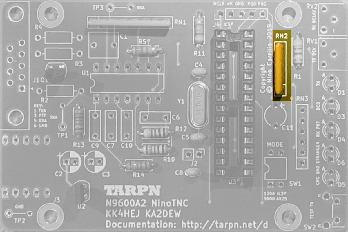 |
 |
|||
| 16 | RN3 | 5 resistor 180ohm resistor network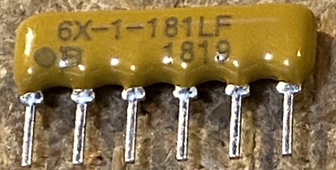 |
Pin 1 is identified by the square around the hole on the PCB and the dot near the end pin on the component.
See the prior RN1 step.
See schematic symbol below.
This provides an in circuit resistance to limit the LED current for 5 LEDs 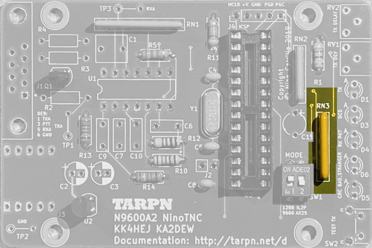 |
 |
|||
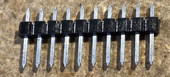
| 17 | SW1 | 2 position dip-switch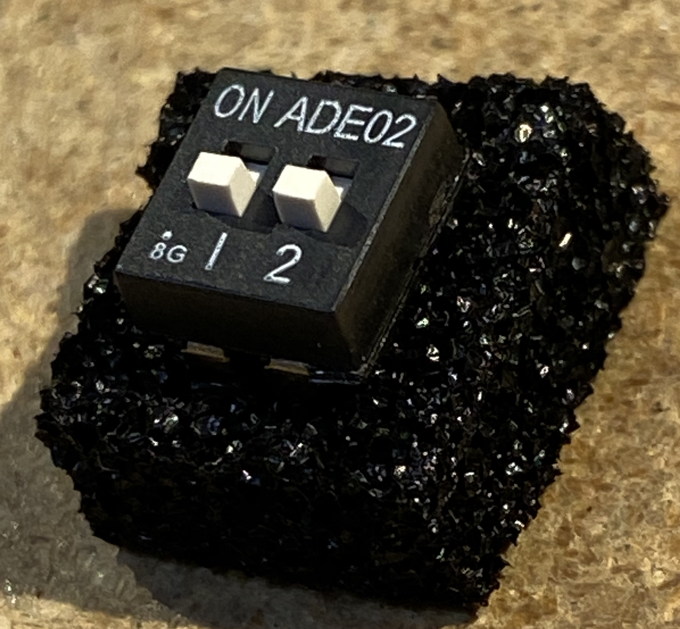 |
Each switch is a separate circuit.
These switches and the 47K pull-down resistors drive two separate inputs on the CPU to select options. If the switch is closed, the switch puts the VCC into the CPU's GPIO input. If the switch is open, the resistor pulls the GPIO to ground. 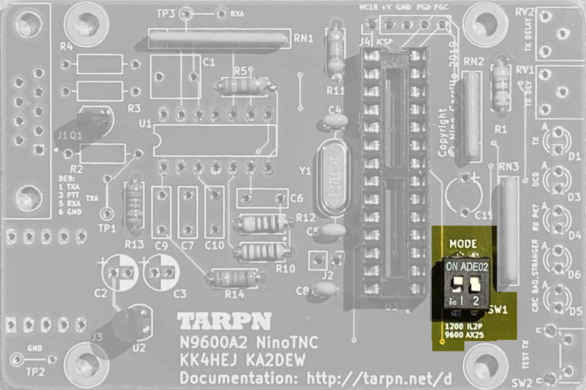 |
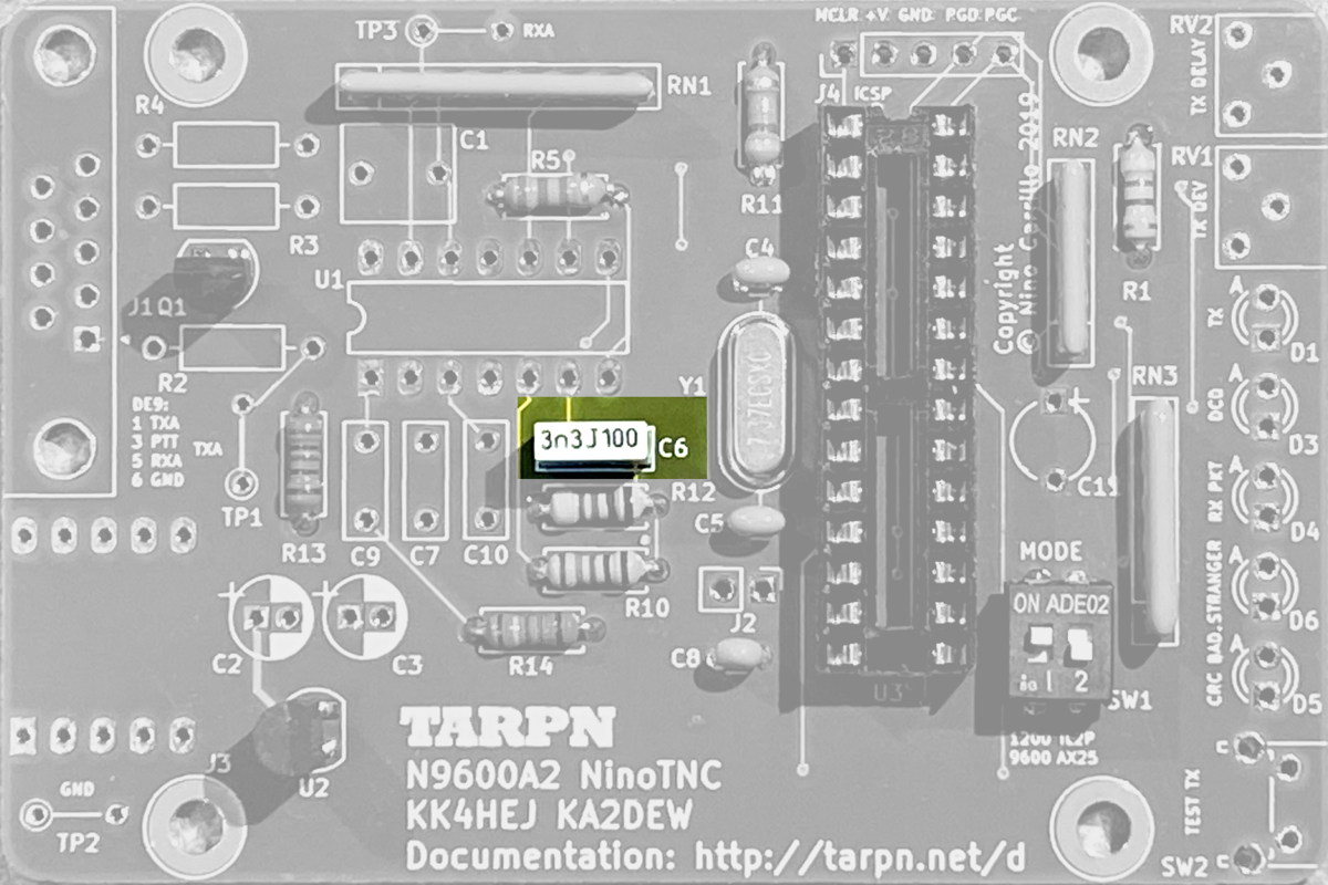
| 18 | C6 | 3300pf [metal] film capacitor radial leads 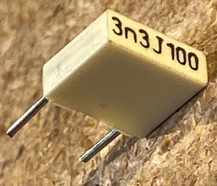 |
This is part of the feedback loop in the 2nd stage of the transmit data output.
 |
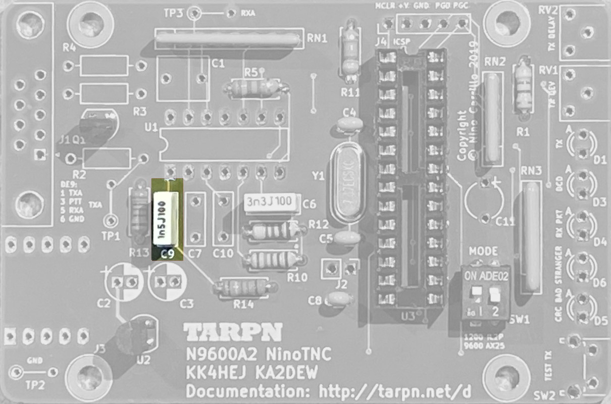
| 19 | C9 | 1500pf [metal] film capacitor radial leads 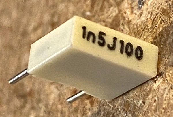 |
This is part of the feedback loop in the 1st stage of the transmit data output.
 |
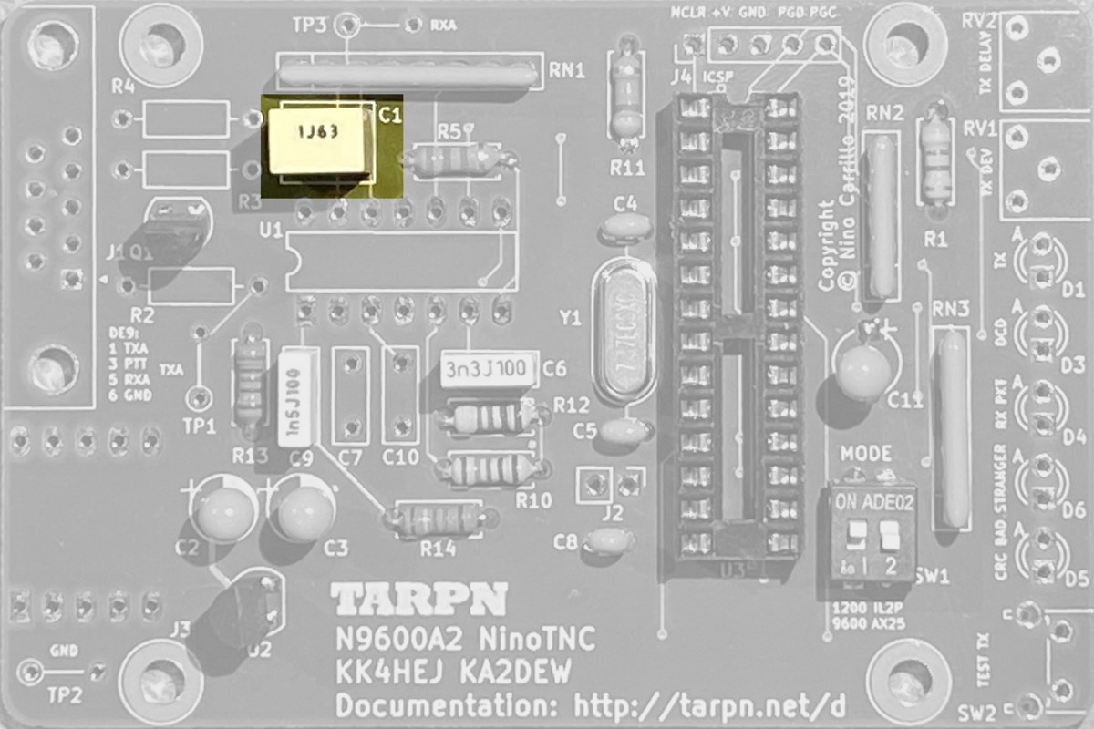
| 20 | C1 | 1uF [metal] film capacitor radial leads  |
This is the capacitive coupling immediately following the DE9 receive data input, before the op-amp receive buffer.
 |
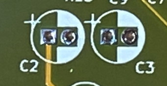
| 21 | C2, C3, C11 | 10uF 10% 16volt tantalum dipped capacitor 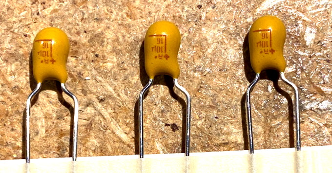
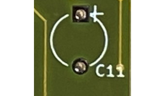 |
Carefully observe values and polarities.
Positive side is marked with a very small plus sign on the part, or a red stripe, and goes into the square solder pad/hole on the PCB.
The silk-screen actually has a microscopic + sign.
C2 is 5v filter on the input to the regulator. C3 is the 3.3v filter on the output from the regulator. C11 is vcap input to the CPU on one side and ground on the other. On the Green prototype A2 board, C2 and C3 leads will have to be reshaped to go into the footprint. This will be fixed on the black production A2 boards. 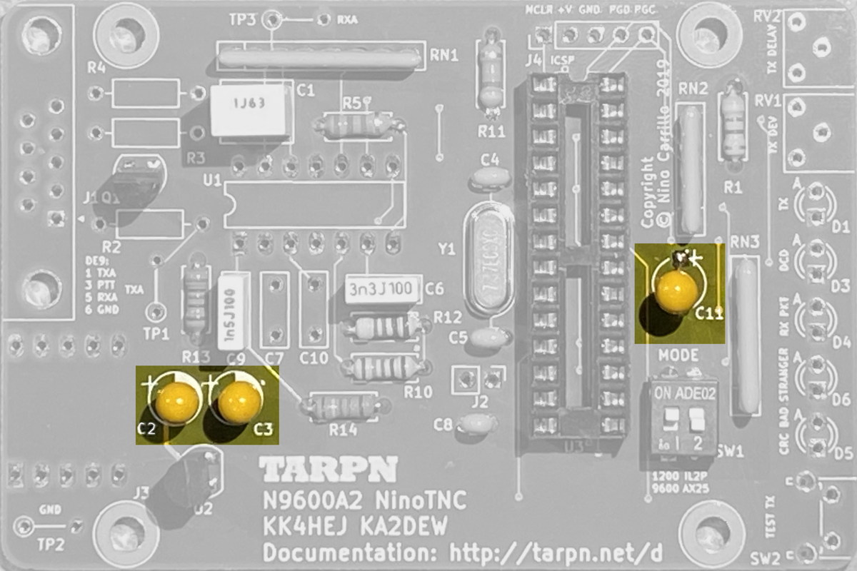 |
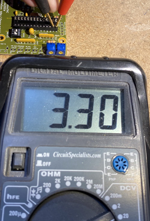
| 22 | RV1 | 10k 1/2watt cermet 1-turn side adjusted trimmer potentiometer. Label=103, 10 * 10**3 = 10000 ohms.
 |
Place in holes so screwdriver adjustable part faces the edge of the board.
This adjusts the Tx Audio level 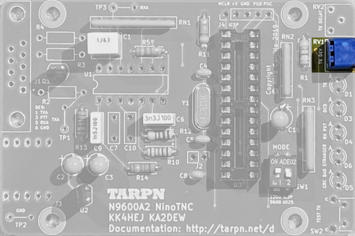 |
 |
|||
| 23 | RV2 | 100k 1/2watt cermet 1-turn side adjusted trimmer potentiometer. Label=104, 10 * 10**4 100000 ohms.
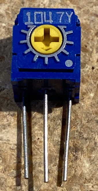 |
Place in holes so screwdriver adjustable part faces the edge of the board.
This unit adjusts the TXDELAY. The potentiometer is read by an AtoD port on the CPU which figures out how much delay between PTT and starting the packet based on the AtoD reading it gets.  |
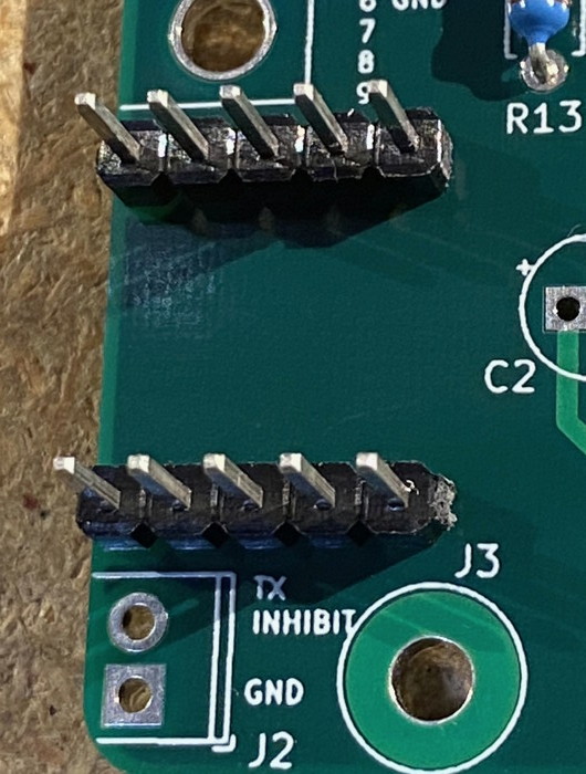
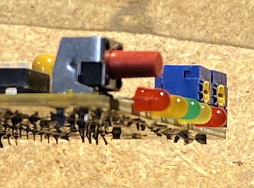
| 26 | SW2 | side facing push button switch labelled TEST TX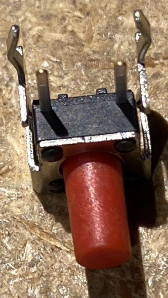 |
Pressing this button connects a GPIO input to the CPU to VCC.
Releasing lets the GPIO be pulled to ground through RN2 47k ohm pull-down resistor. Mount so switch button faces off the edge of the board, directly away from the J3-pins in step 24. 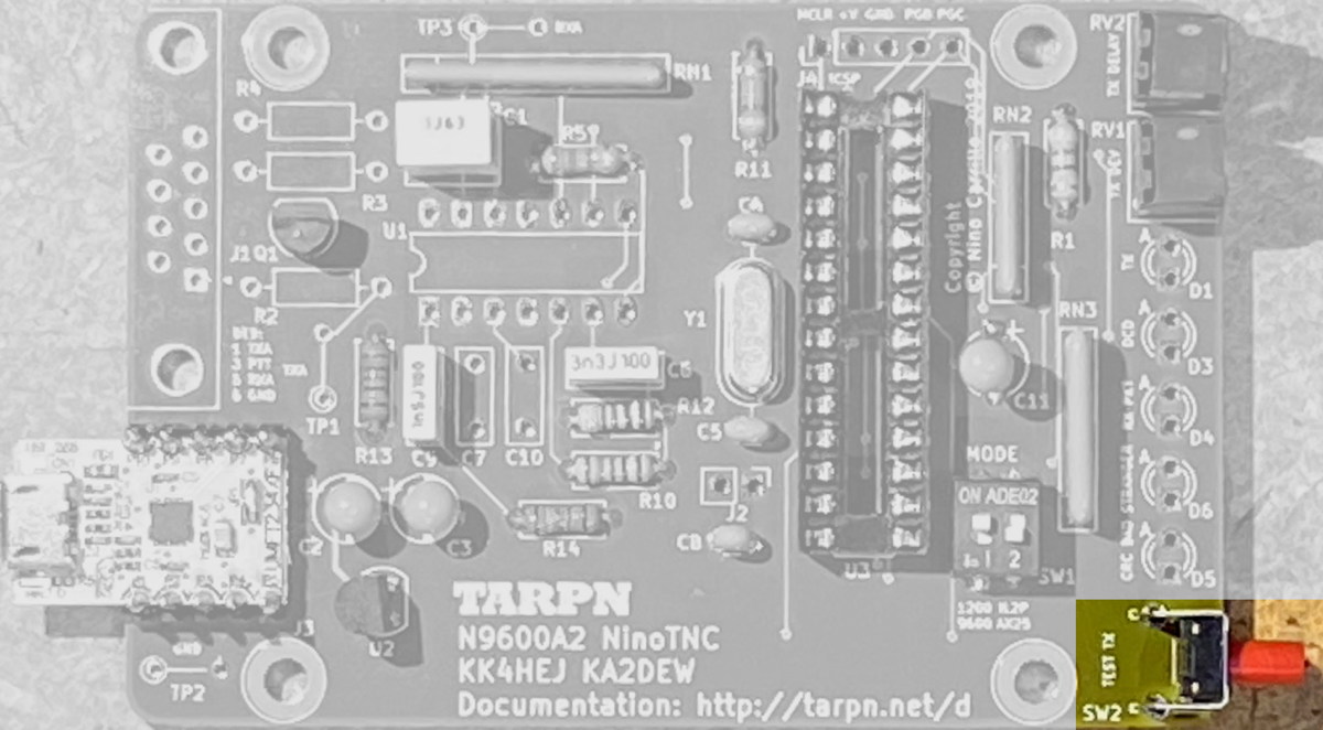 |
|
Over the next several steps you're going to bend the leads of 5 LEDs.
Our goal is to have the LEDs pointing off the end of the board in between SW2 and RV1, lined up with and below SW2's push button pin.
The leads need to be just long enough before the bend such that the LED lays over the end of the board and just misses the end of the board.
This is the crankiest part of this kit construction. Please try to be careful. Here is a photo of my first attempt to get this right: |
|||
 |
|||
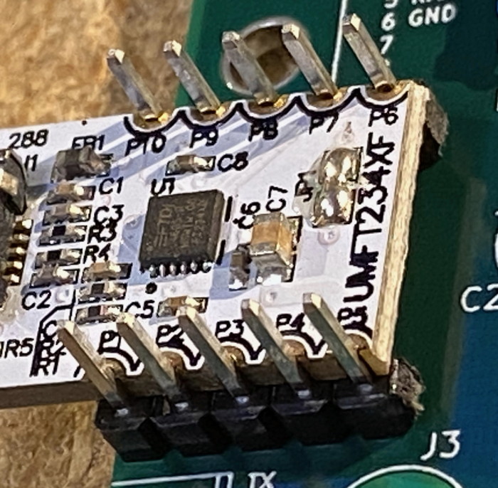
| 27 | D1 and D5 | LED Red diffused part#160-1139-ND 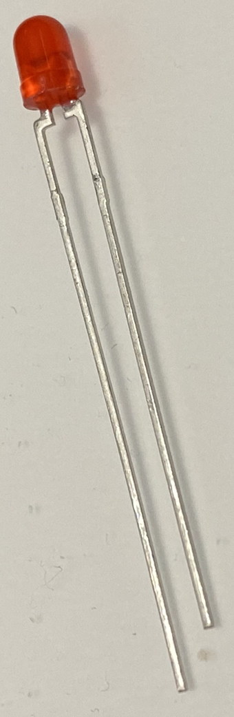 |
PTT and CRC error LED This part is polarized. We're going to bend the leads on the LEDs before insertion. We need to get the length of wire, between the LED body and the bend, to be exactly the proper length. First, notice that the LEDs have a long and a not-so-long lead. The short lead goes into the square hole. You need to make sure to not mistake the leads as you bend them. Hold the LED up against the FTDI board such that the body of the LED is on the down side of the FTDI board and the LEDs poke up past the entrance into the USB socket. 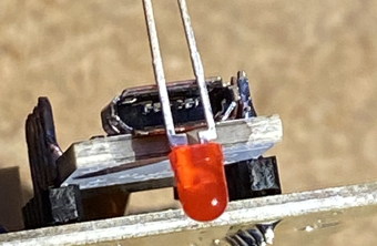
Now, looking at the end of the FTDI board as in the above photo, with the LED's leads facing 'up', make sure the short lead is to the left, and long to the right. Another way of looking at it is the short lead is on the Q1 side USB connector and the long lead is toward the U2 side of the connector. In your fingers, the body of the LED is pressed up into the underside of the white FTDI board. The wires are flush up against the USB socket. Now, bend the two leds back over the top of the USB socket. 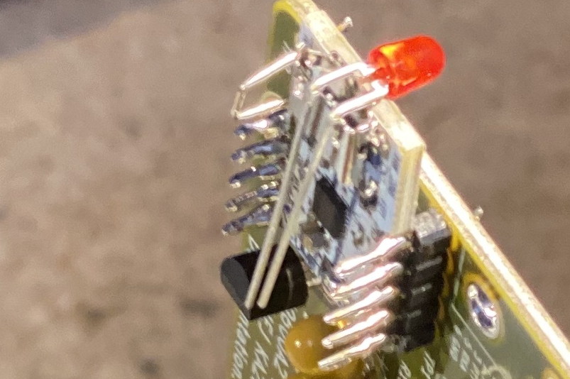
It may help to hold the PCB in the soft grip of a clamp. Insert the LED into the hole marked D1, again making sure the short lead goes into the square hole. After inserting the leads through the holes, lay the LED over the edge of the board. Now pull and spread the leads out, on the back side of the board, and try to keep the LED folded to the edge of the board as you solder. Repeat the bending procedure with the 2nd red LED, soldering it into position D5. 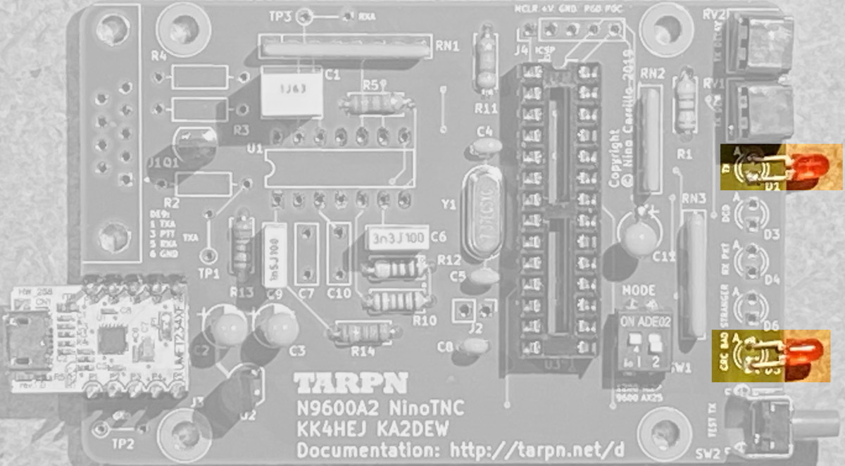 |
| 28 | D3 | LED Yellow diffused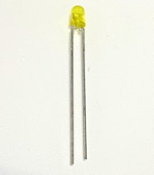 |
Data Carrier Detect LED This part is polarized. The shorter lead goes in the square hole Do the same procedure as you did in the earlier step. |
| 29 | D4 | LED Green Diffused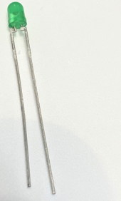 |
OK packet LED This part is polarized. The shorter lead goes in the square hole Do the same procedure as you did in the earlier step. |
| 30 | D6 | LED Orange Diffused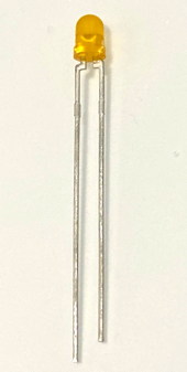 |
Stranger detected This part is polarized. The shorter lead goes in the square hole Do the same procedure as you did in the earlier step. |
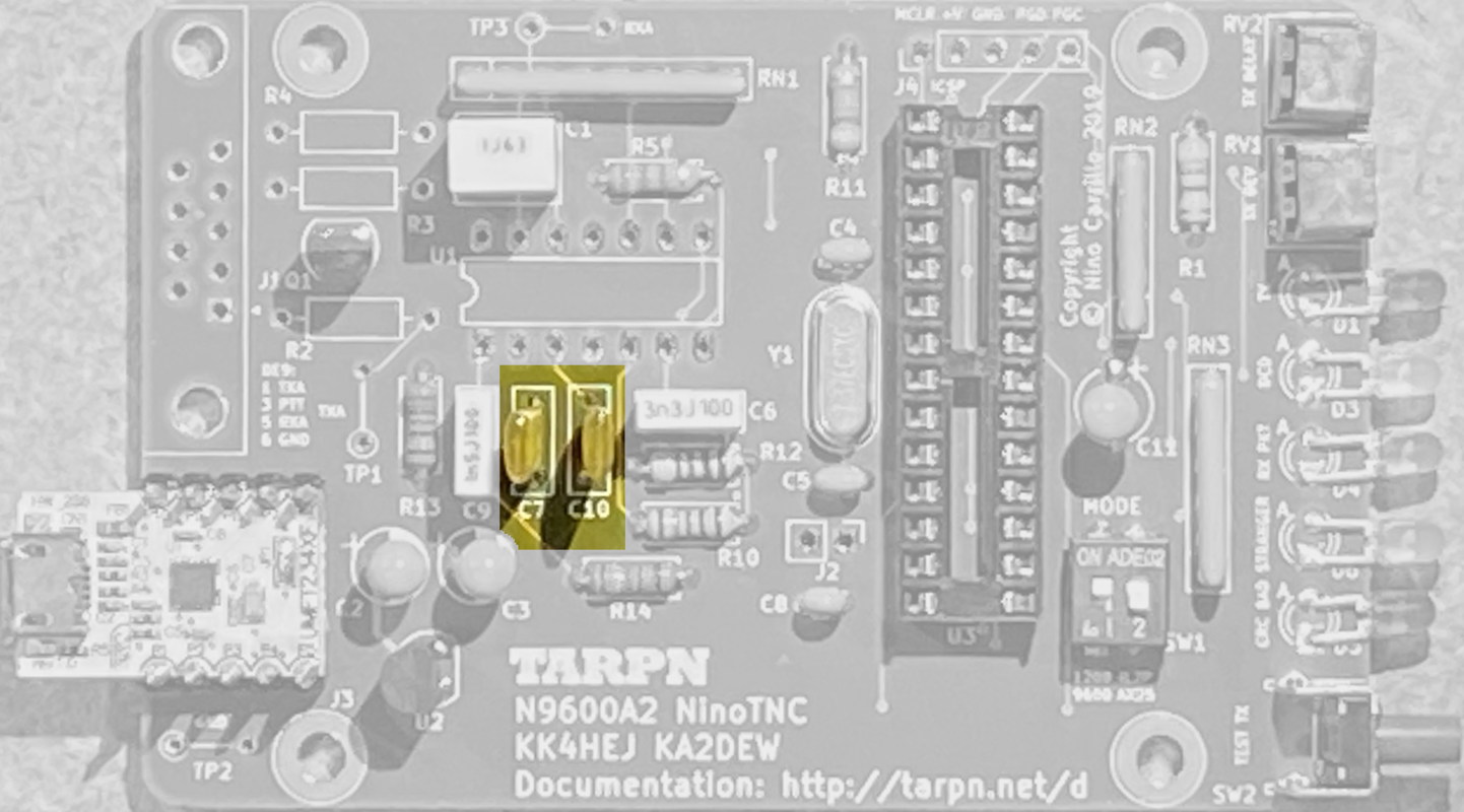
| 31 | C7, C10 | 1200 pF 50v |
polyester film capacitor
 |
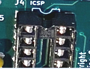
| 32 | Test points TP1, TP2, TP3 | These are loops of scrap wire. 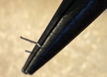 |
Test points for receive audio, transmit audio and ground.
See pix below for installation. 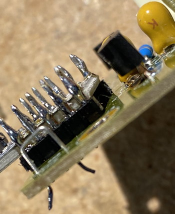
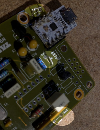 |
| 33 | L1, L2, L3 (proto-A2 had R2, R3, R4) |
Note: for 1200 baud microphone audio use, replace L2 with a 20K to 47K resistor. See note at top of page
Optional Ferrite beads 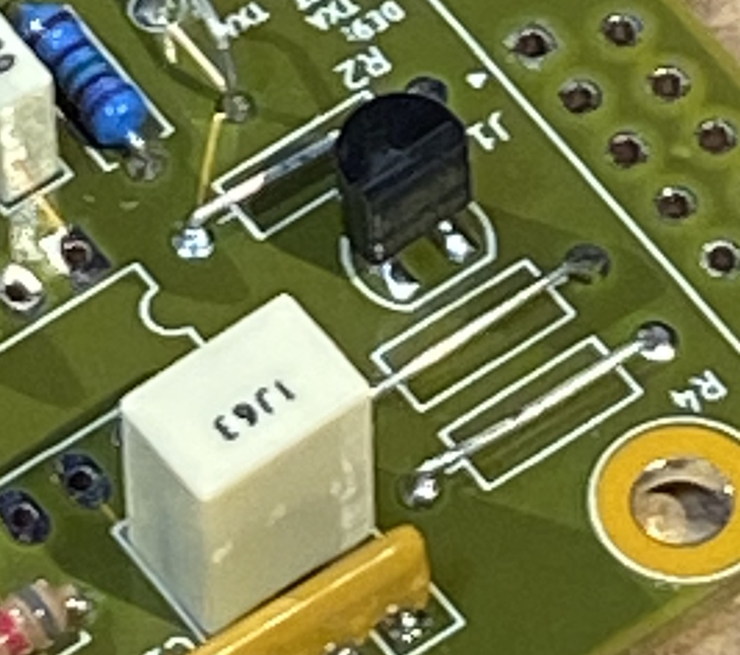 |
For typical builds, use scrap wire.
See pix below for installation. 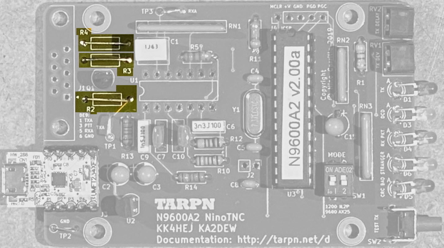 |
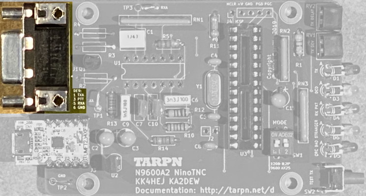
| 34 | J1 | DE9 connector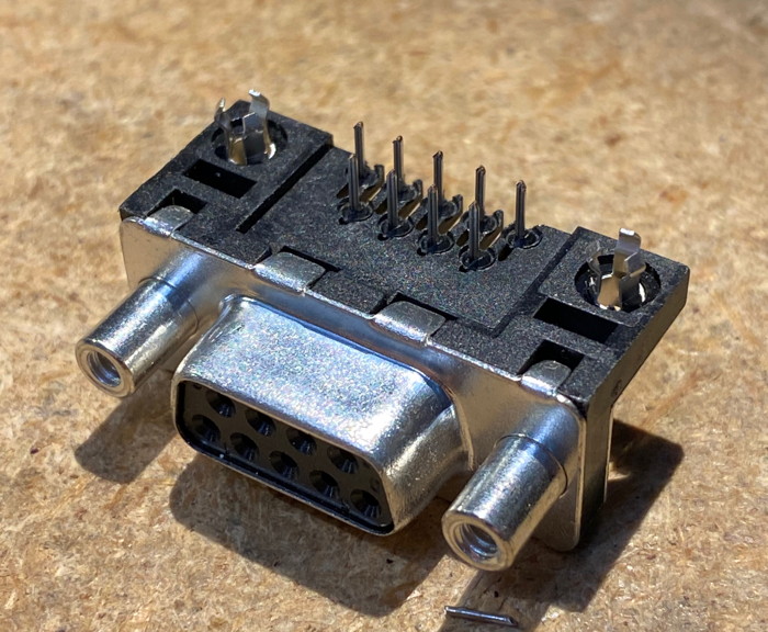 |
Audio and PTT to the transceiver
 |
| 35 | U1 | MCP6004
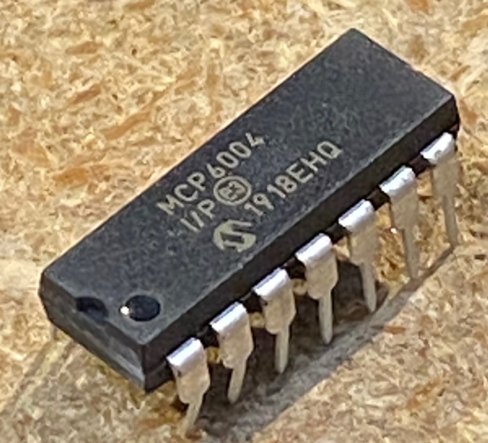 |
Install the MCP6004 quad op-amp Integrated Circuit without a socket.
The pins will have to be bent a little to fit.
Since the PCB is now rather crowded, and since the pin bending isn't really obvious,
I recommend test-fitting the IC on the back of the PCB, and then when you get the pins bent as needed, move around to the front of
the PCB and insert the op-amp where it needs to be.
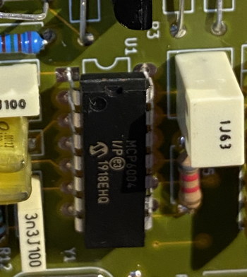
Make sure the half-moon shaped end lines up with the PCB as shown in the photos. This is a quad-package op-amp (operational amplifier) used to buffer the receive AF data signal from the radio and to condition and buffer the transmit AF data signal to the radio. 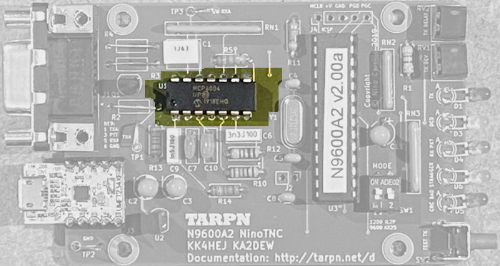 |
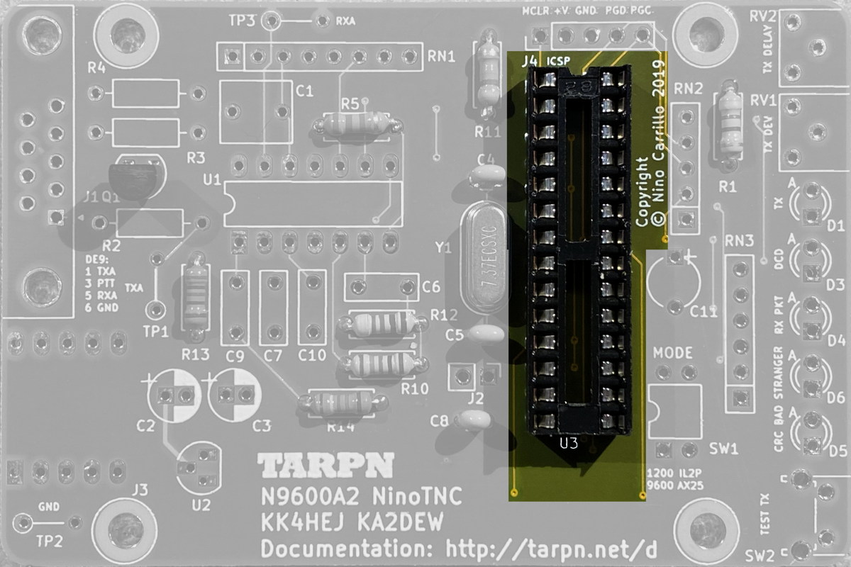
| 36 | U3 | dsPIC33EP256GP502
 |
Install the CPU into its socket.
The pins will have to be bent a little to fit.
Do not screw up.
Make sure the half-moon shaped end lines up with the PCB as shown in the photo. Half moon is pointed away from the TARPN logo.  |