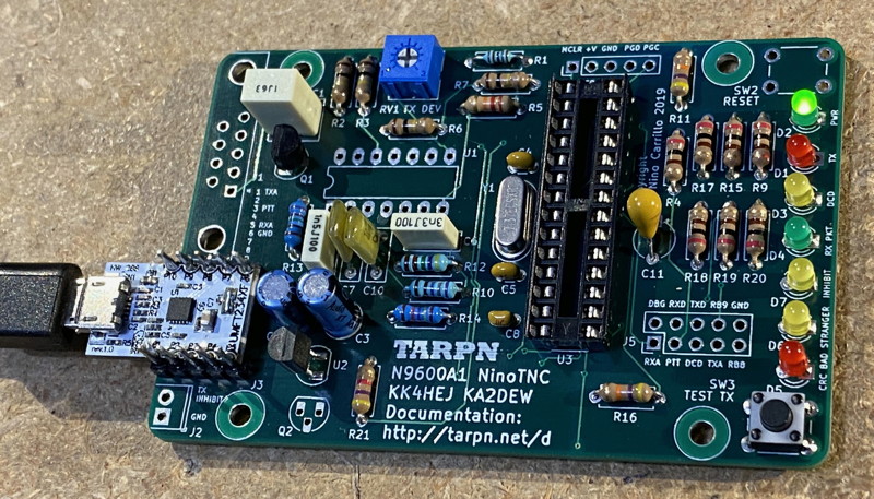
| home | builders | Search |
| builders ➜ TARPN Kits and Projects ➜ NinoTNC N9600A ➜ N9600A1 Assembly |
Some of the images on this page can be enlarged and opened in a new browser tab by clicking on them.
| ⇒ All parts are inserted from the silk-screened side of the board, i.e. from the side on which the white writing is printed. |
| ⇒ Except where specifically noted, all two pin components are non-polorized so you can put the part onto the board with the pins in either hole. |
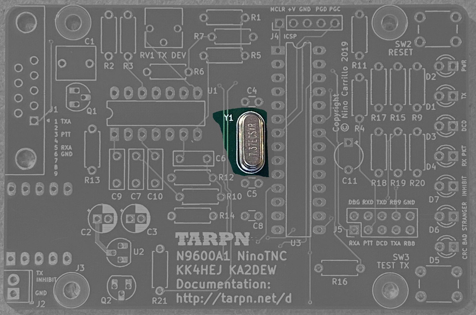
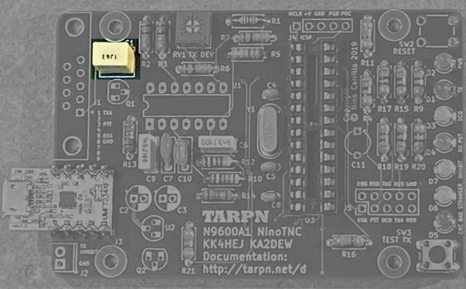
| 1 | Y1 | 7.3728 MHz crystal
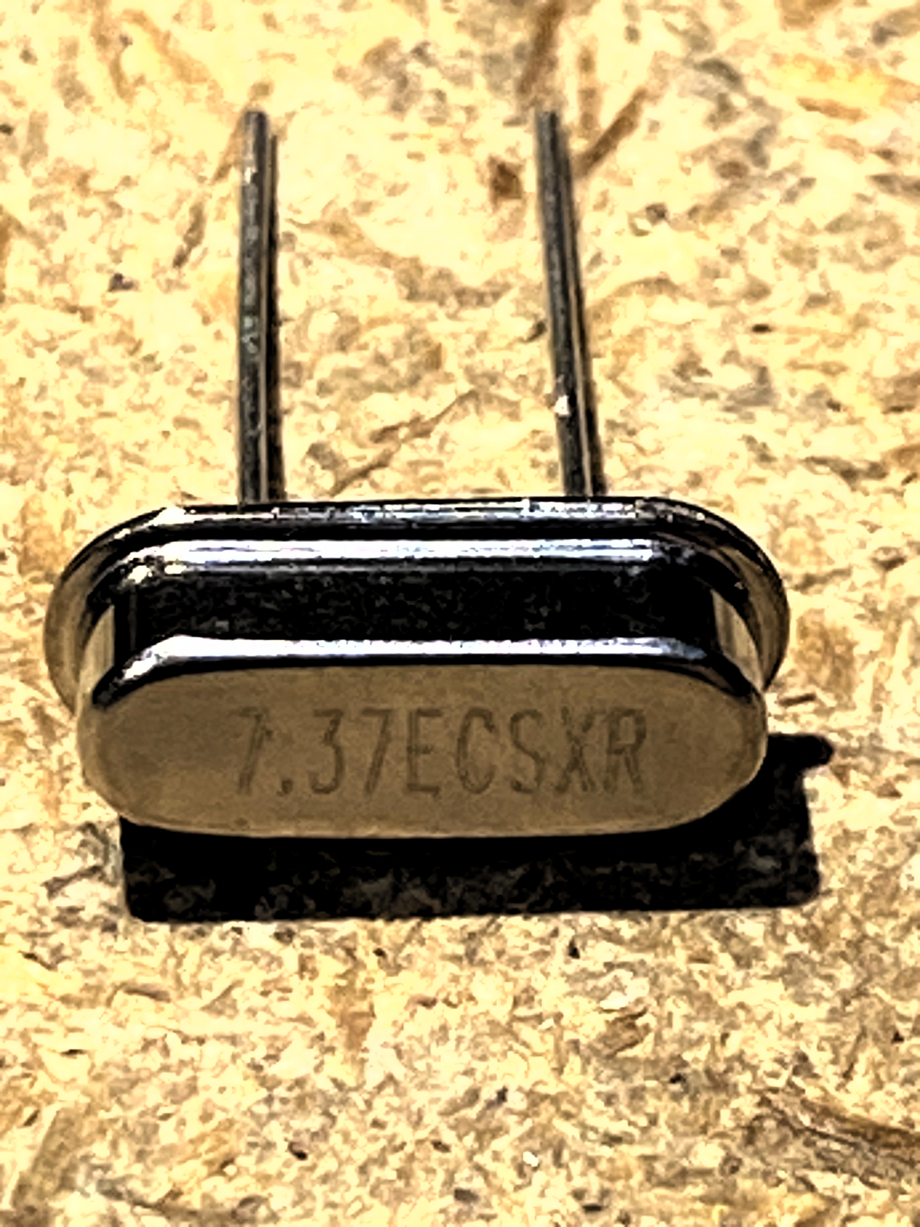 |
The crystal will have some code on it containing the numbers 7.37
 |
| 2 | R4, R9, R15, R17, R18, R19, R20 | 200 ohm 5% resistors
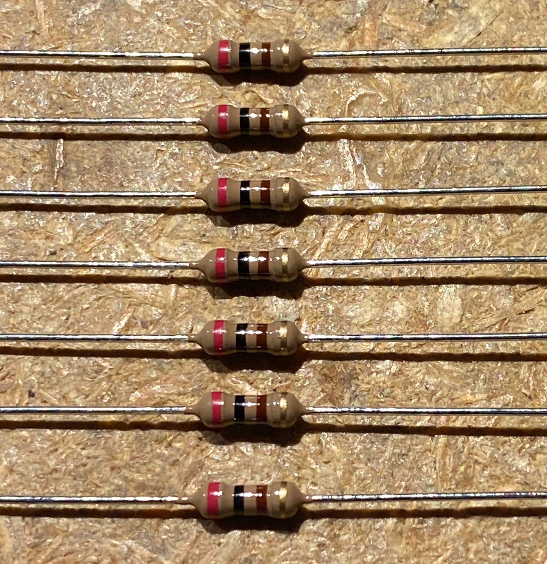 |
These are the LED current limit resistors.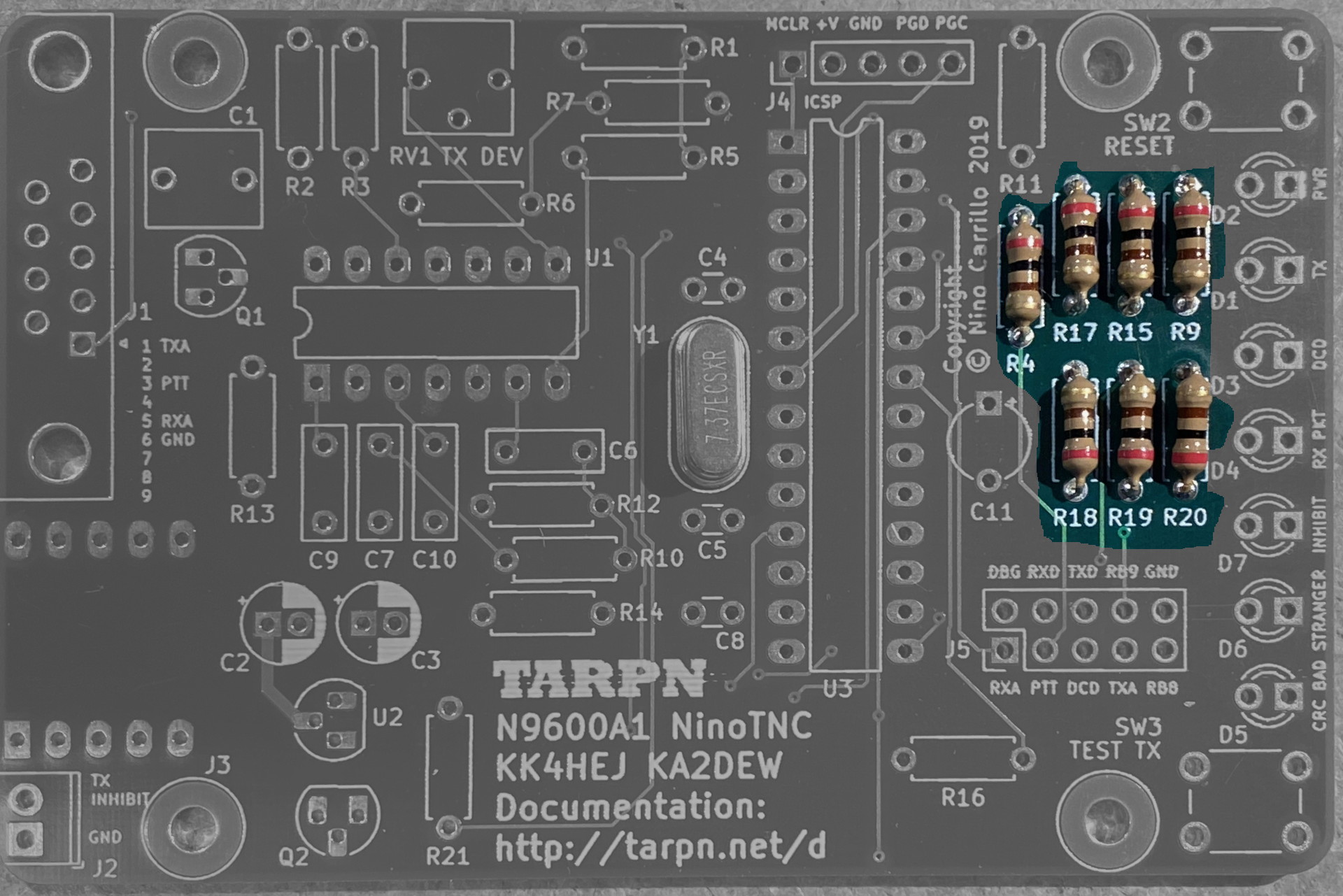 |
| 3 | R2, R3, R6, R7 | 100K ohm 5% resistors
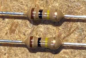 |
These are used in pairs to generate a voltage halfway between ground and 3.3v. This is used for as bias voltage for two different op-amp elements of U1..
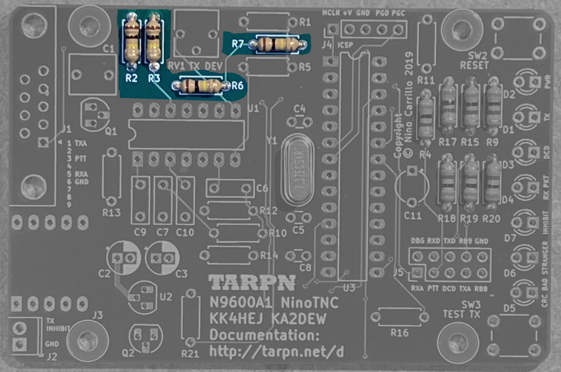 |
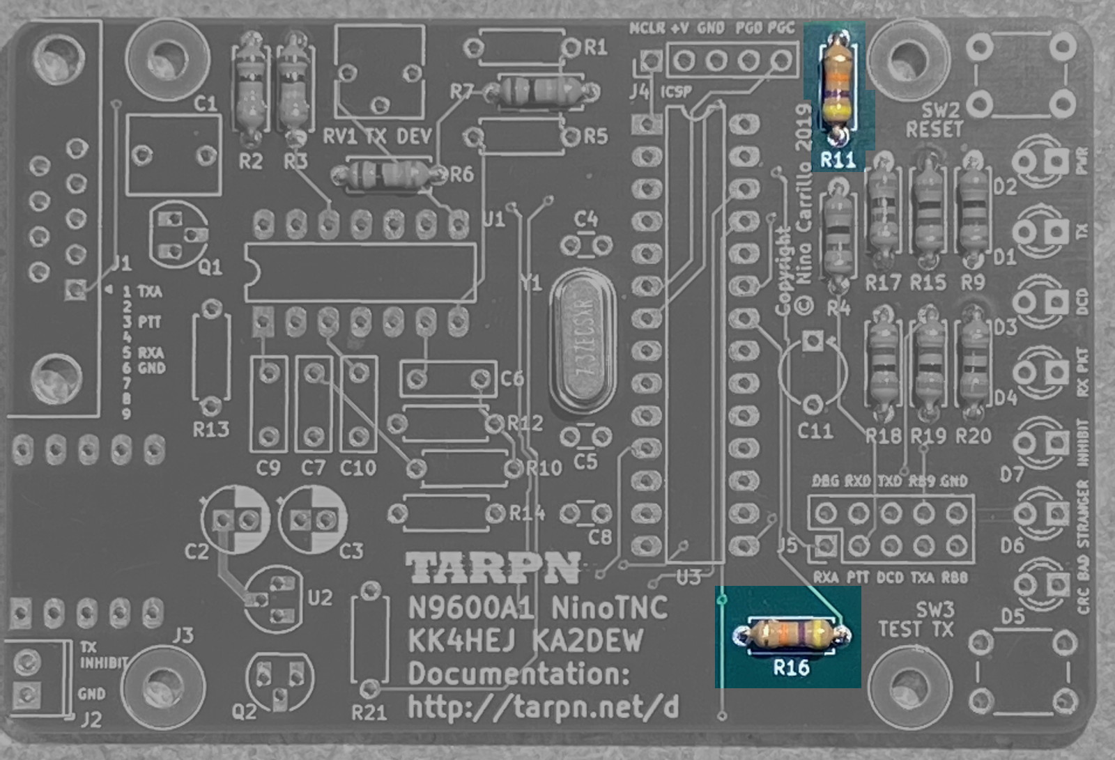
| 4 | R11, R16 | 47K ohm 5% resistors
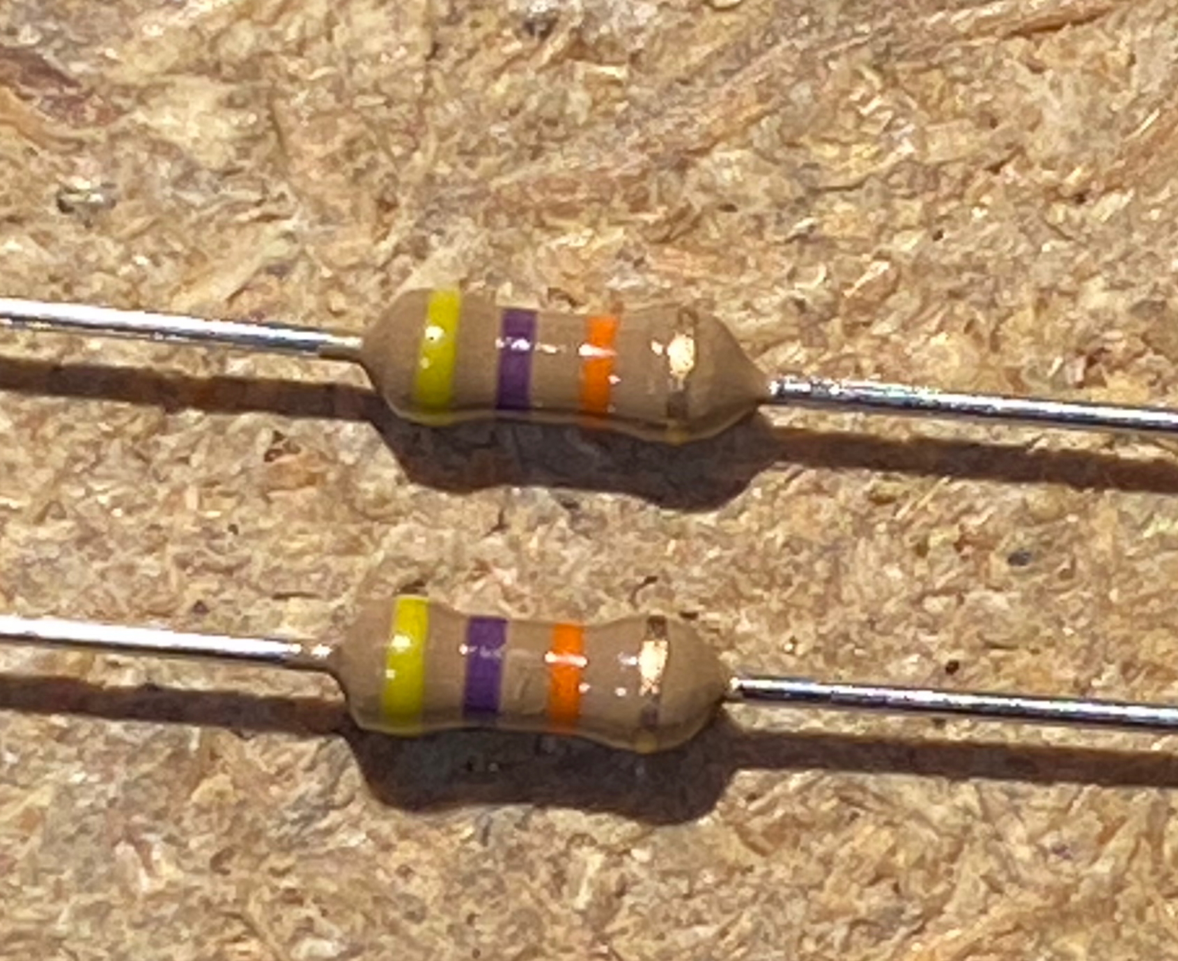 |
R11 turns off the MCLR input to the CPU. R16 is a pulldown to the Transmit Test button.
 |
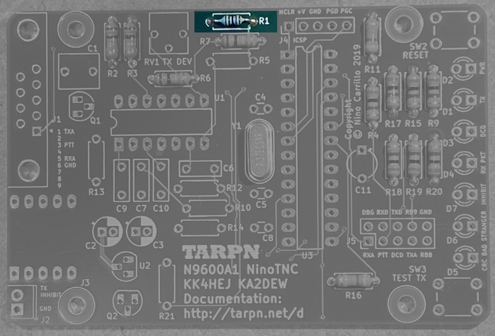
| 5 | R1 | 1.1K ohm 1% precision resistor 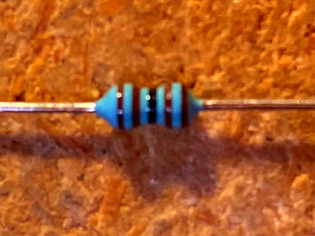 |
This is a low-end-limit to the Deviation adjust. It doesn’t need to be a precision resistor and it might not be in your version.
 |
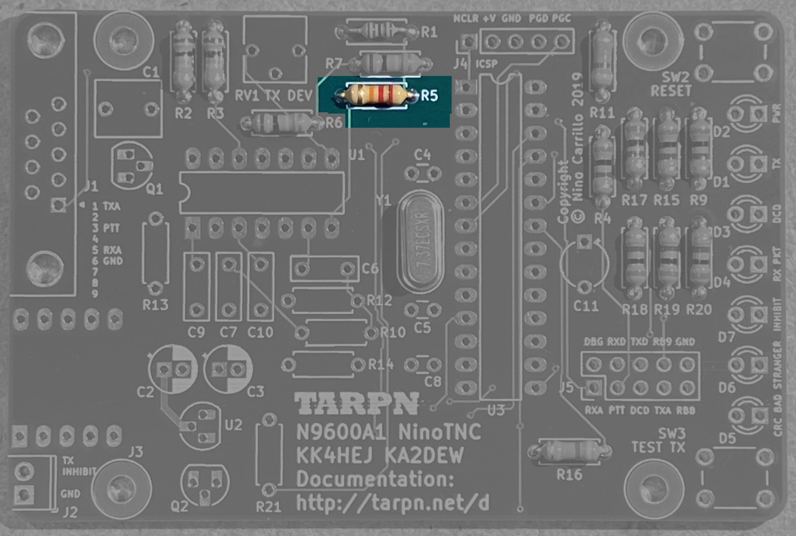
| 6 | R5 | 22K ohm 5% resistor Note: May use 1% substitute 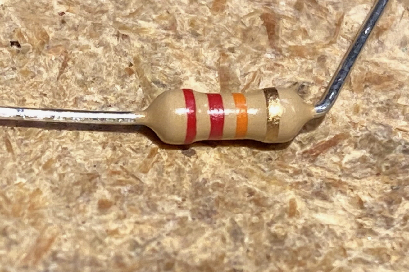 |
In the TX-data/audio path between U1B and U1C op amp devices.
 |
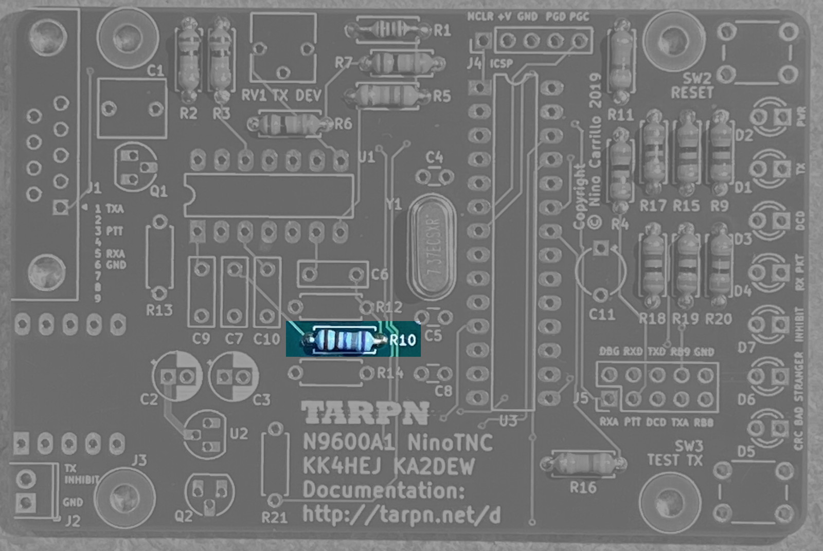
| 7 | R10 | 7.87ohm 1% precision resistor 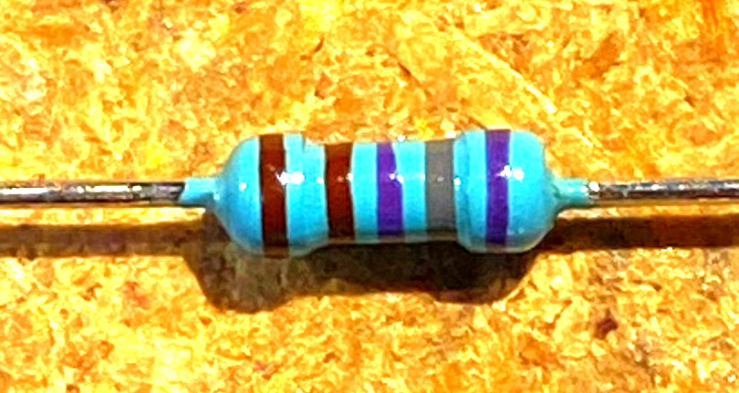 |
This resistor is in the input and feedback loop for the 2nd op-amp stage in the TX-data/audio path.
 |
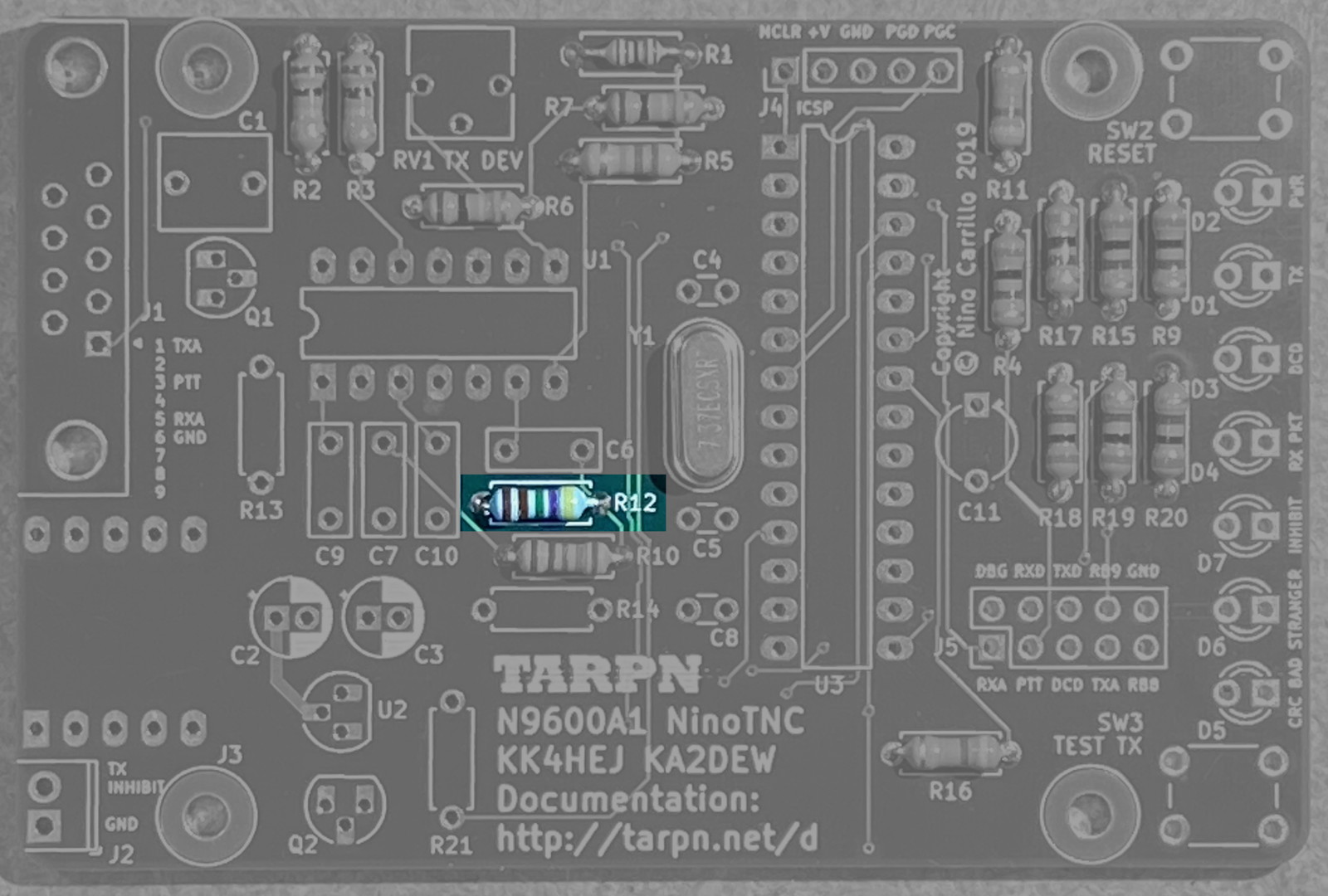
| 8 | R12 | 4.75Kohm 1% precision resistor 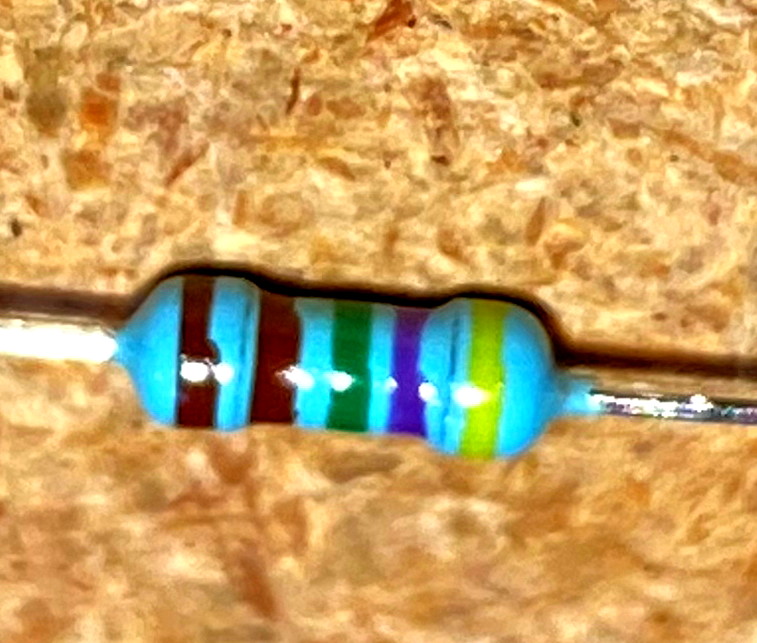 |
This resistor is in the audio path between the 1st and 2nd op-amp stage in the TX-data/audio path.
 |
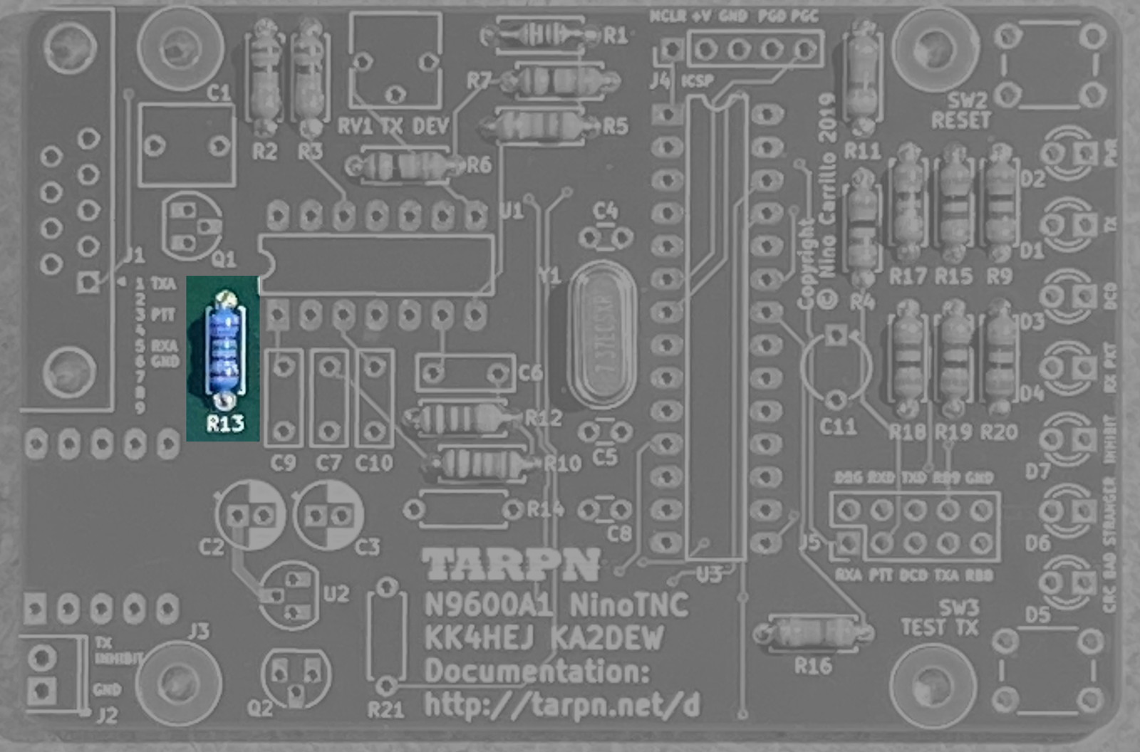
| 9 | R13 | 7.15Kohm 1% precision resistor  |
This resistor is in the input and feedback loop for the 1st op-amp stage in the TX-data/audio path.
 |
| 10 | R14 | 14.7Kohm 1% precision resistor 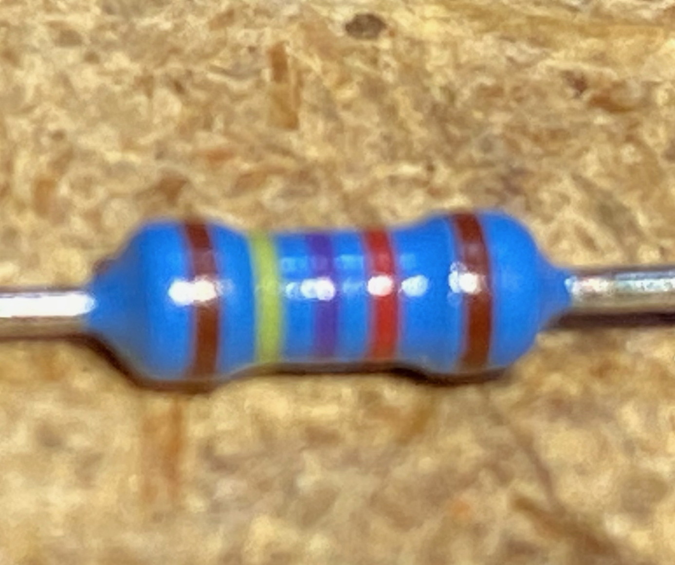 |
This is part of the amplifier circuit for the 1st op-amp stage in the transmit data circuit.
 |
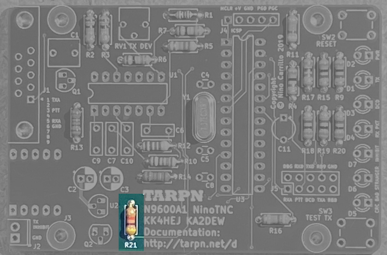
| 11 | R21 | 4.7Kohm 5% resistor
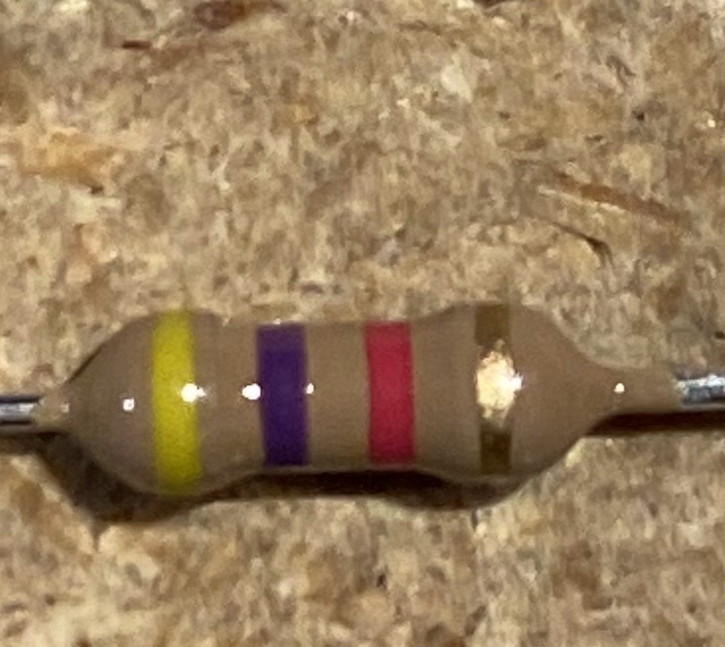 |
This is a pull-up on the TX Inhibit bus. The CPU will drive this bus low when receiving. TNCs are tied together using this bus when they are on the same ham-band. This prevents other TNCs on the same band at the same site from interfering with each other.
 |
| 12 | C8 | 0.1uF ceramic radial capacitor  |
This ceramic radial capacitor provides power supply filtering and glitch reduction on the CPU’s main power input.
 |
| 13 | C4, C5 | 18pf ceramic radial capacitor 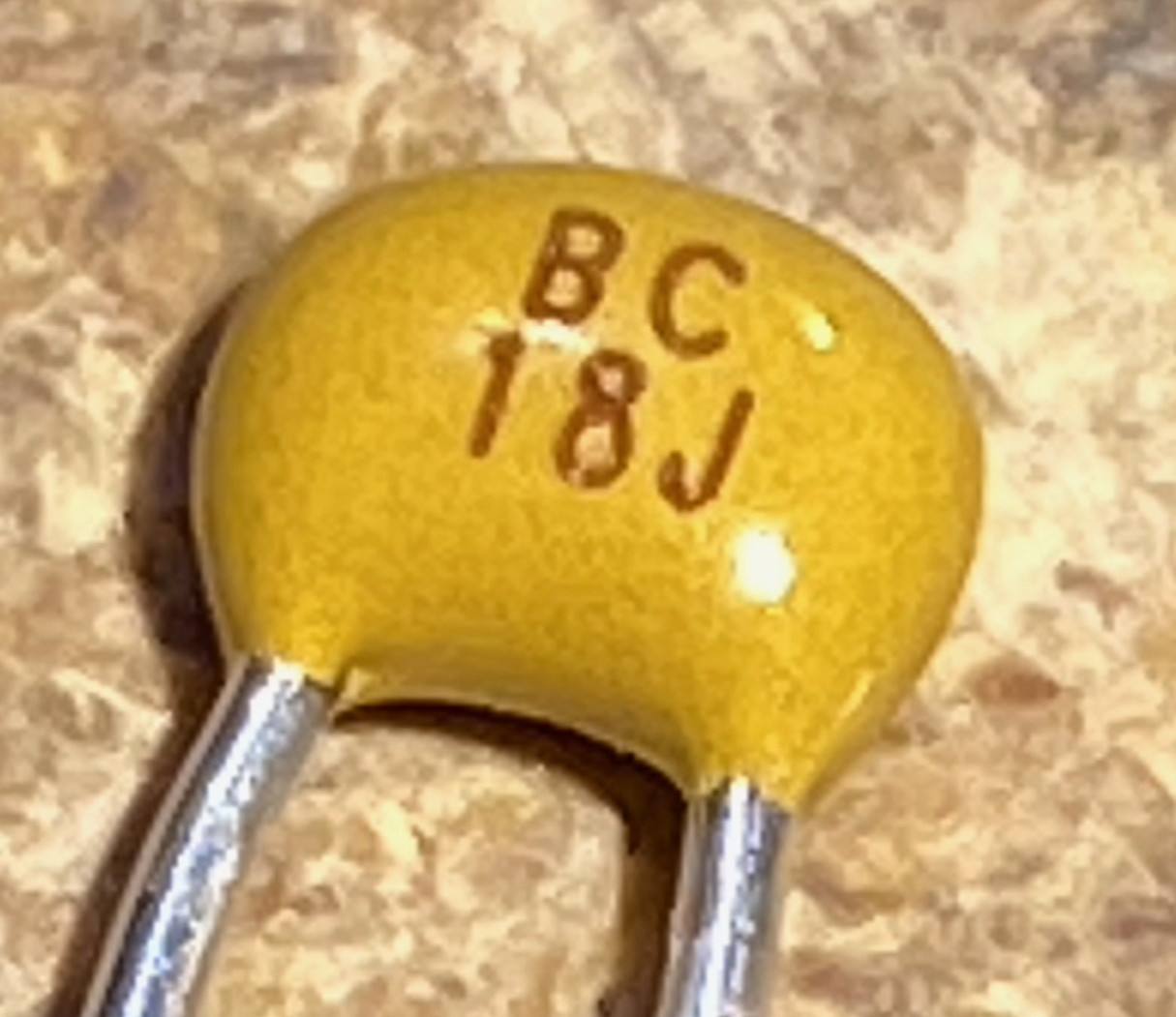 |
These ceramic radial capacitors are part of the crystal oscillator circuit. There is one capacitor on each leg of the crystal between ground and the wire from the crystal to the CPU.
 |
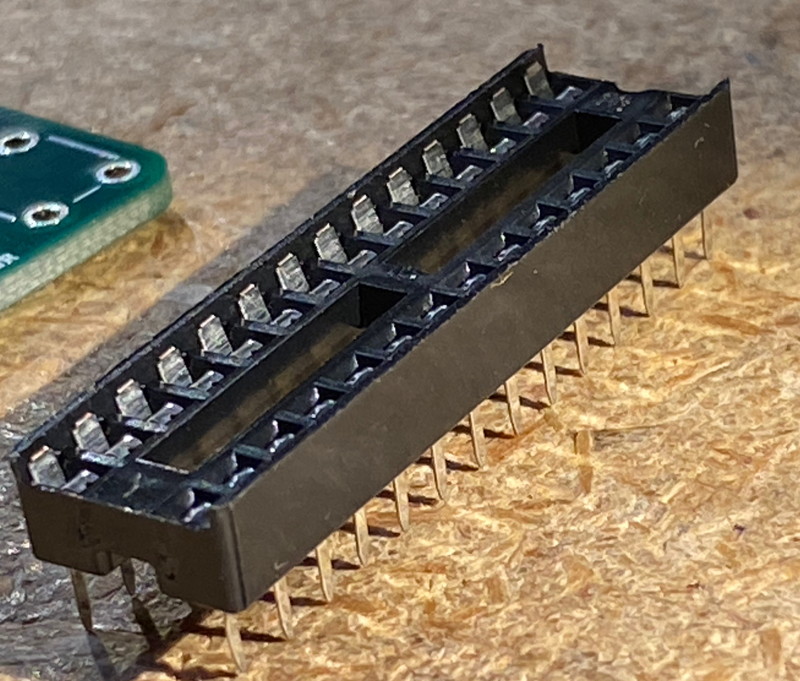
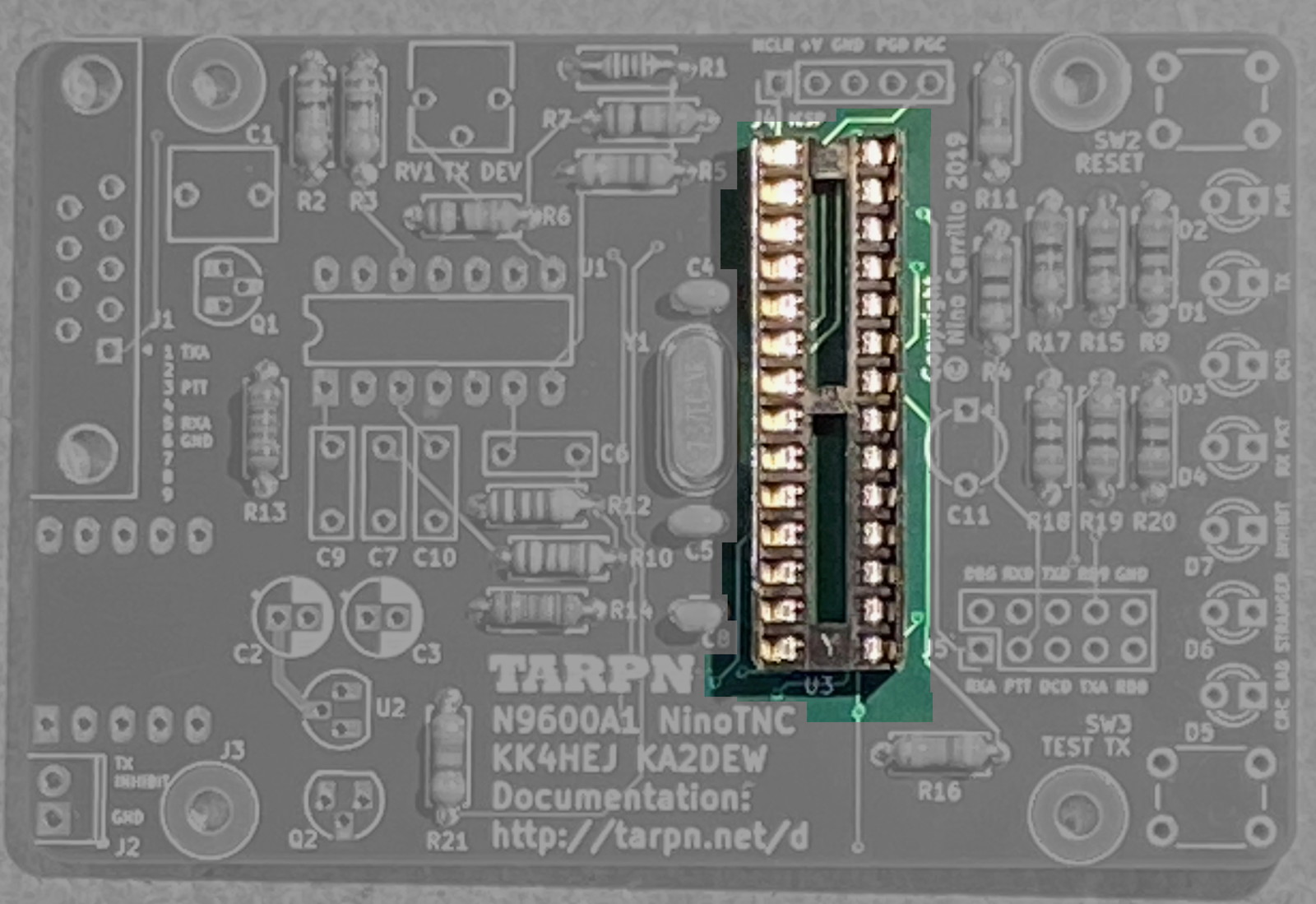
| 14 | socket U3 | 20 pin DIP IC socket
 |
Make sure all pins are straight. Use long-nose plier to fix any that need fixing. Carefully insert into the board with the round half-moon end pointing to match the board.
That will be up from the perspective of this image. Bend two diagonally opposite leads down to the board outward to hold the socket onto the board as you invert the board to solder.
 |
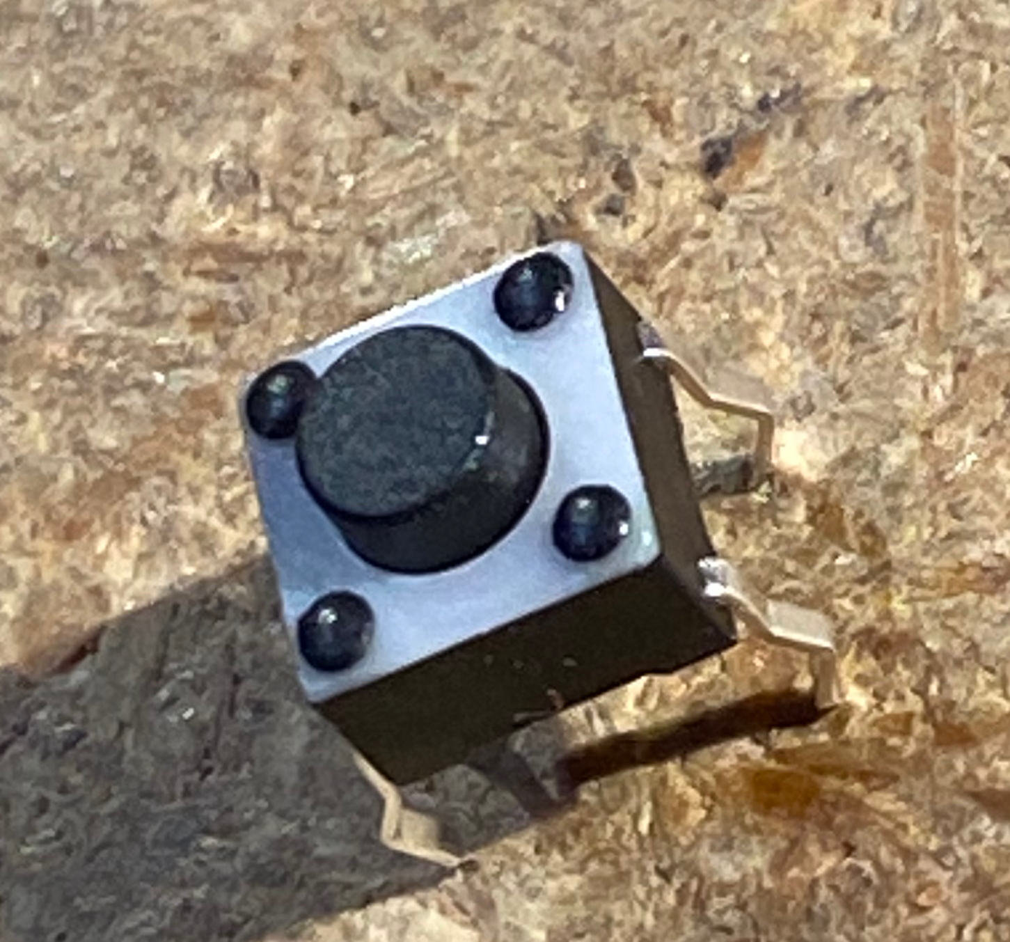
| 15 | SW3 | pushbutton switch
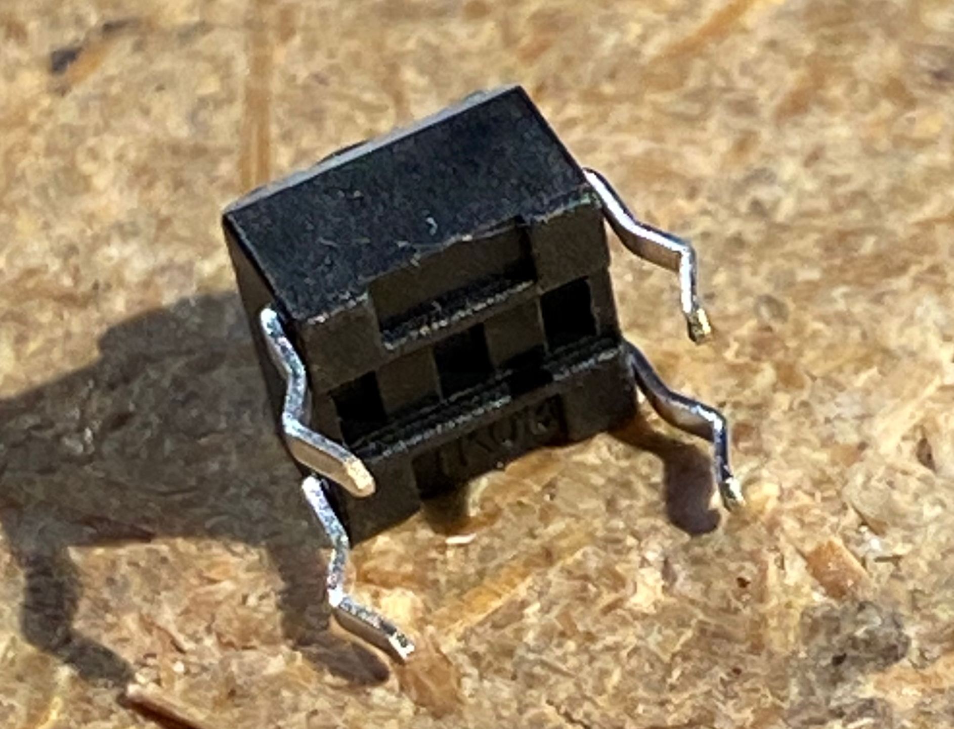 |
TEST-TX Try to get all 4 pins into the holes without bending them. It should fit without any adjustment. Pressing this button tells the CPU to hold the transceiver in transmit. Release to unkey. Note that there is a SW2 RESET pushbutton that we will not be installing. 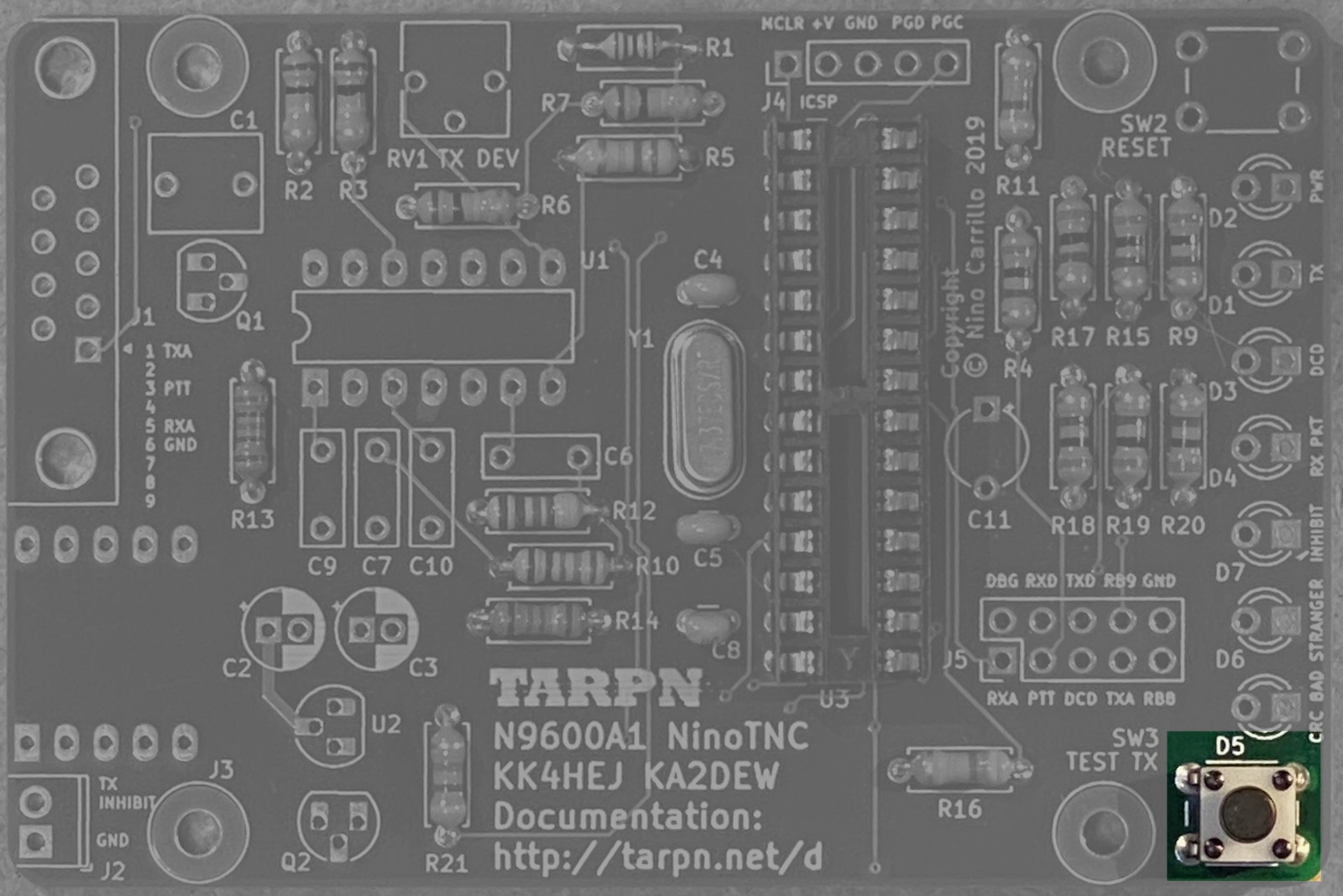 |
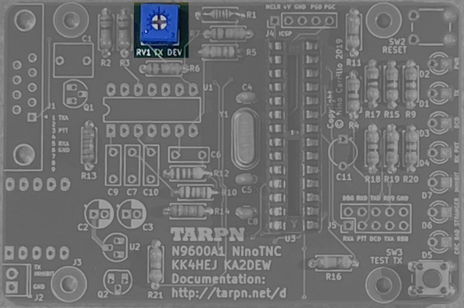
| 16 | RV1 | 10Kohm trimmer potentiometer  |
This is the transmit audio-frequency-signal level adjuster.
 |
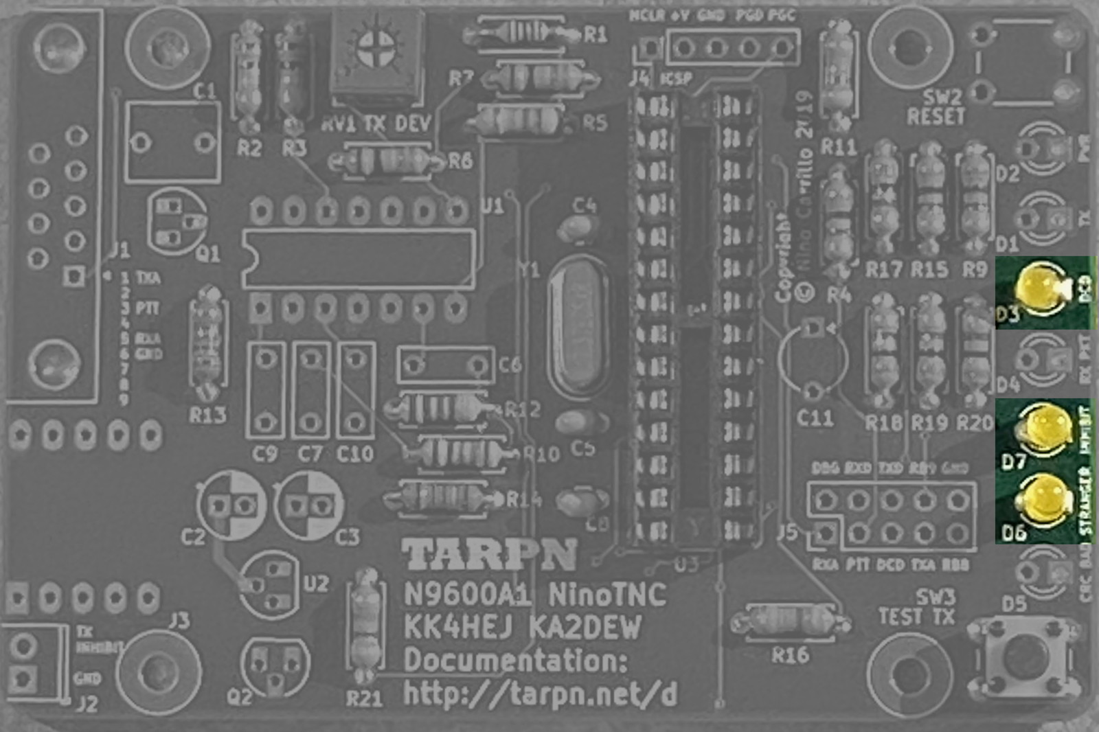
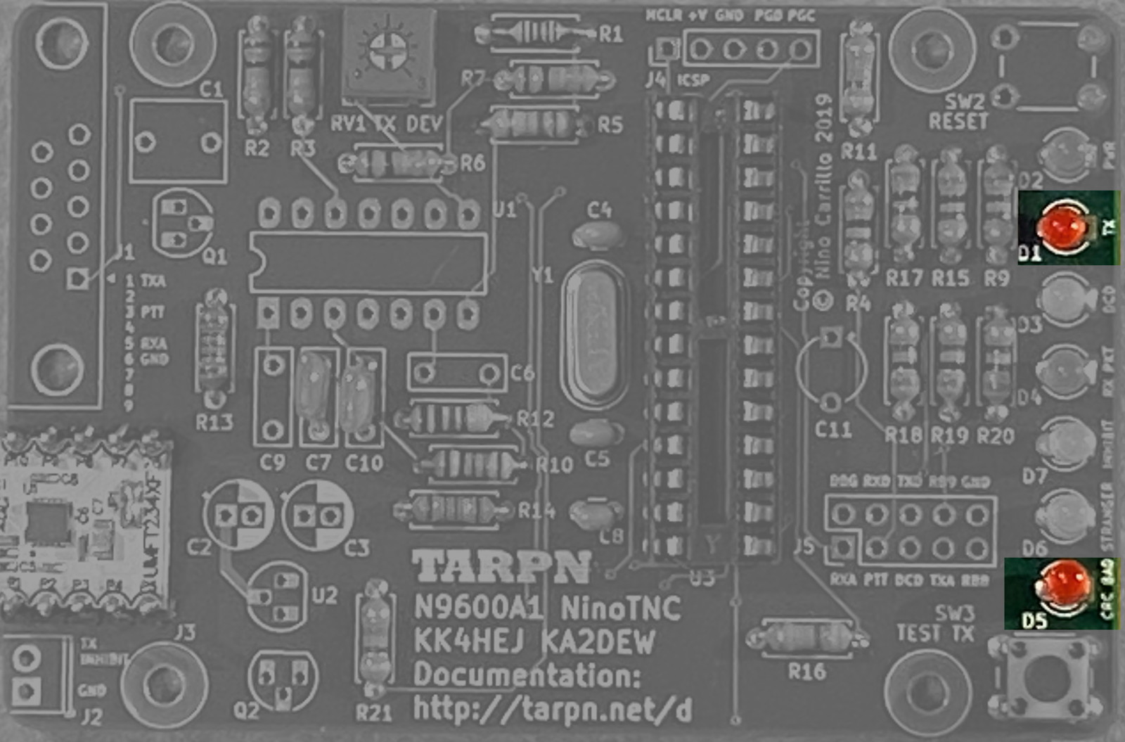
| 17 | D3, D6, D7 | LED, yellow diffused |
These are polarized components. The shorter lead goes in the square hole
 |
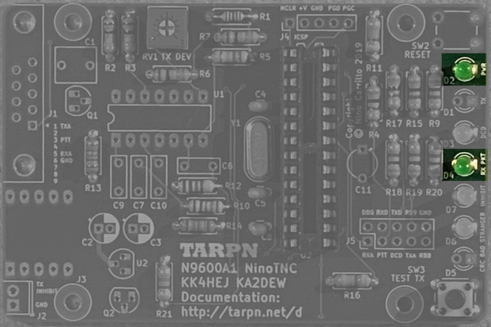
| 18 | D2, D4 | LED, green diffused |
These are polarized components. The shorter lead goes in the square hole!
 |
| 19 | D1, D5 | LED, red diffused 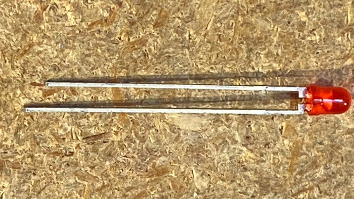 |
These are polarized components. The shorter lead goes in the square hole!
 |
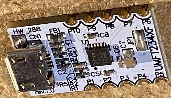
This is the bag the FTDI module comes in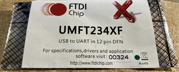
|
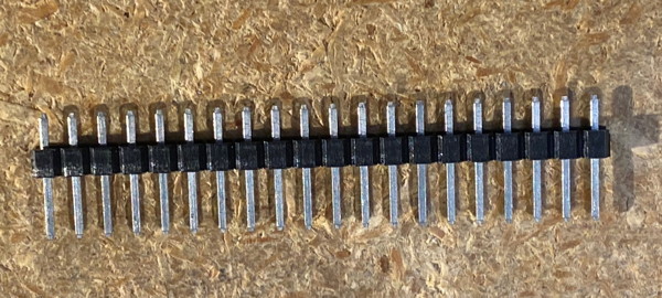
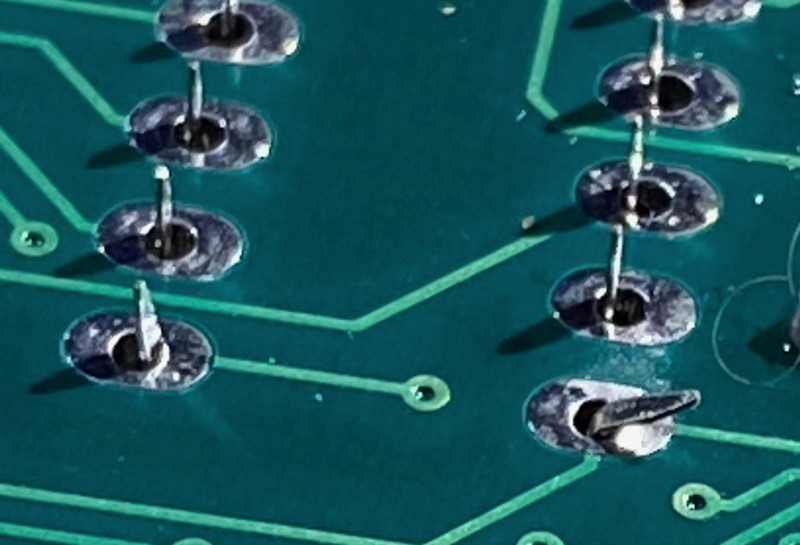
Header pins soldered into place. Now insert the module in between the 10 pins such that the USB socket hangs off the board.
| |
The module is inserted between the pins, ready to be soldered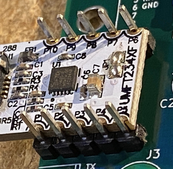
|
The module has been soldered in. Solder is definitely bridging each of the 10 pins to the half-moon on the FTDI board.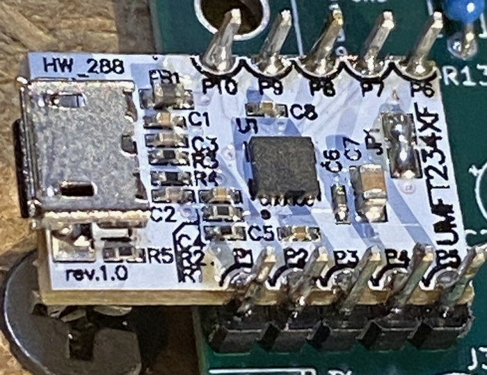
|
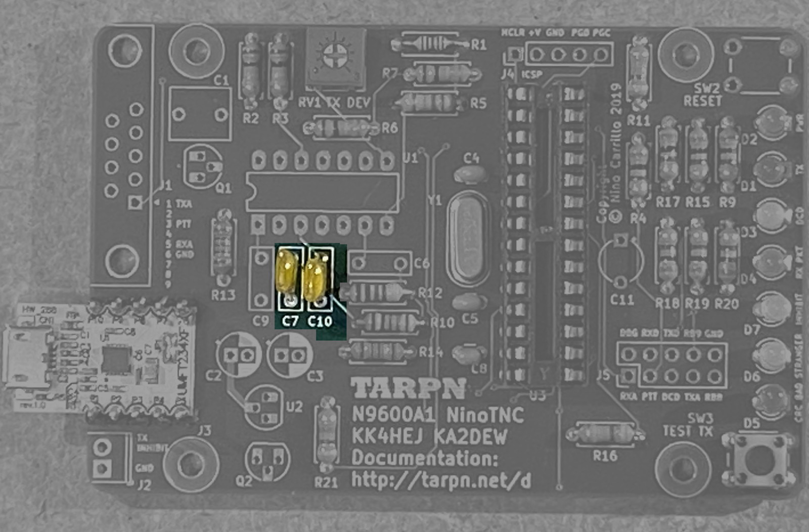
| 21 | C7, C10 | 1200pf [metal] film capacitor radial leads 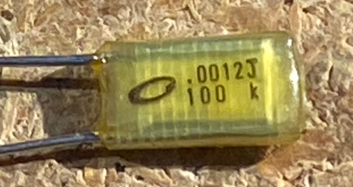 |
C7 and C10 are part of the input circuit for two of the op-amps in the transmit data output.
 |
| 22 | C6 | 3300pf [metal] film capacitor radial leads 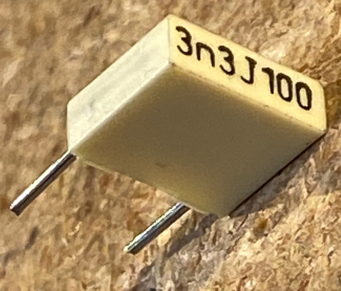 |
This is part of the feedback loop in the 2nd stage of the transmit data output.
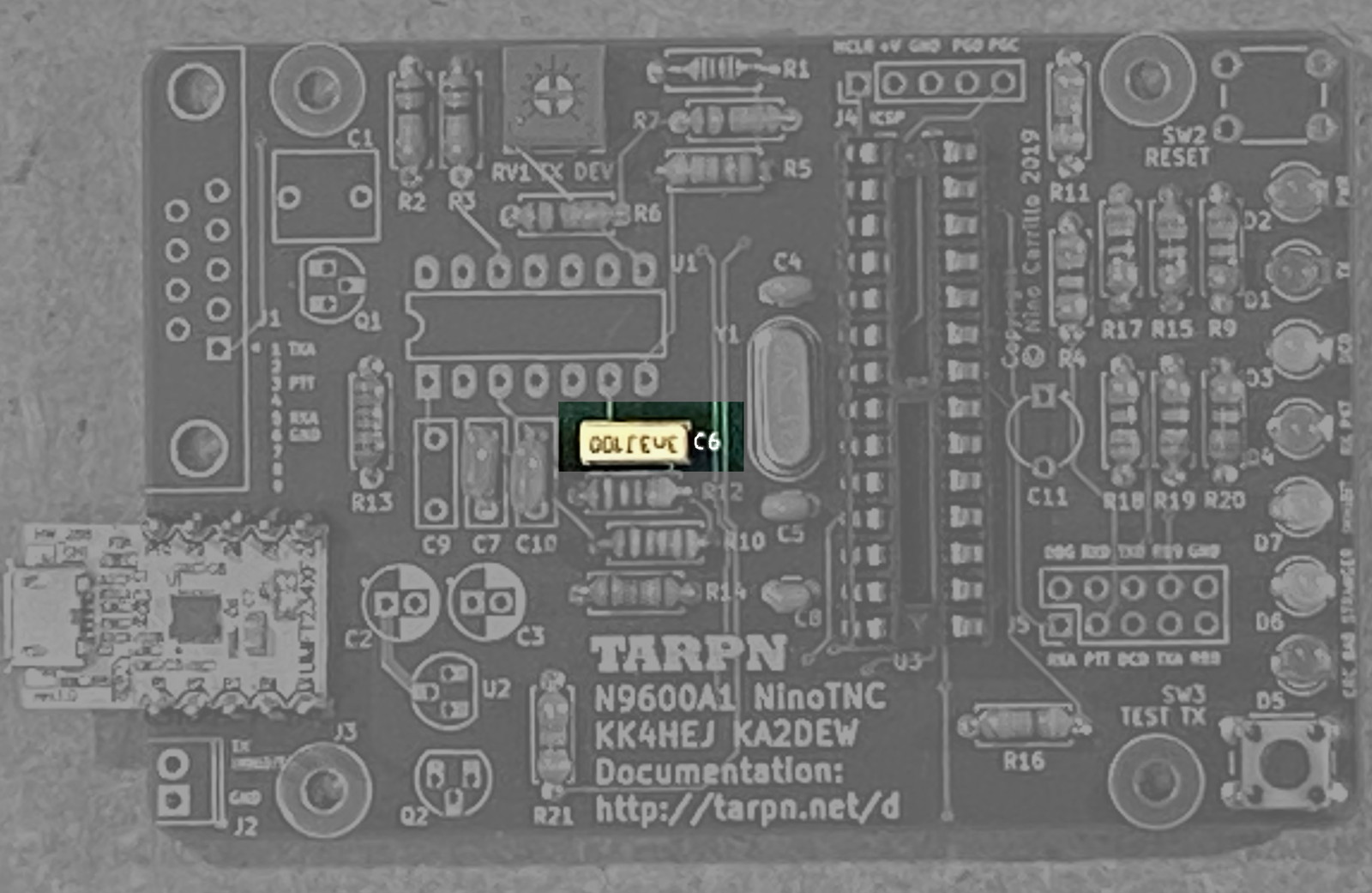 |
| 23 | C9 | 1500pf [metal] film capacitor radial leads 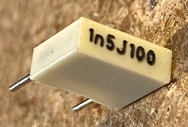 |
This is part of the feedback loop in the 1st stage of the transmit data output.
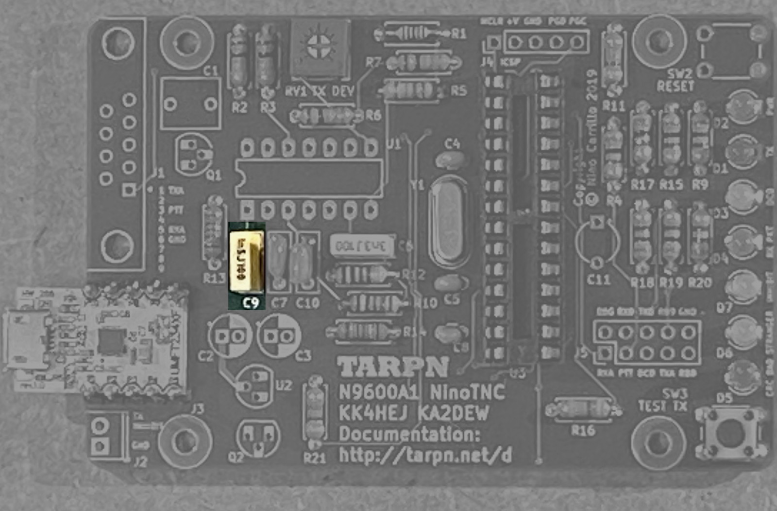 |
| 24 | C1 | 1uF [metal] film capacitor radial leads 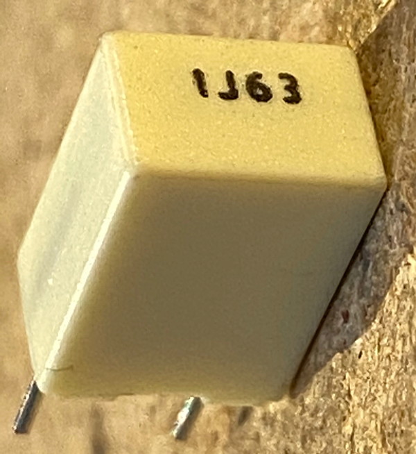 |
This is the capacitive coupling immediately following the DE9 receive data input, before the op-amp receive buffer.
 |
| 25 | C2 | 10uF 15volt aluminum electrolytic capacitor, radial leads 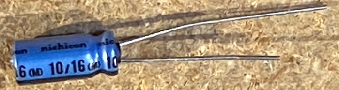 |
Carefully observe values and polarities. Cathode (negative) is marked with a black stripe and goes into the round solder pad/hole on the PCB.
The silk-screen actually has a microscopic + sign. Put the --- side away from that.
This is the 5v input filter capacitor before the regulator. 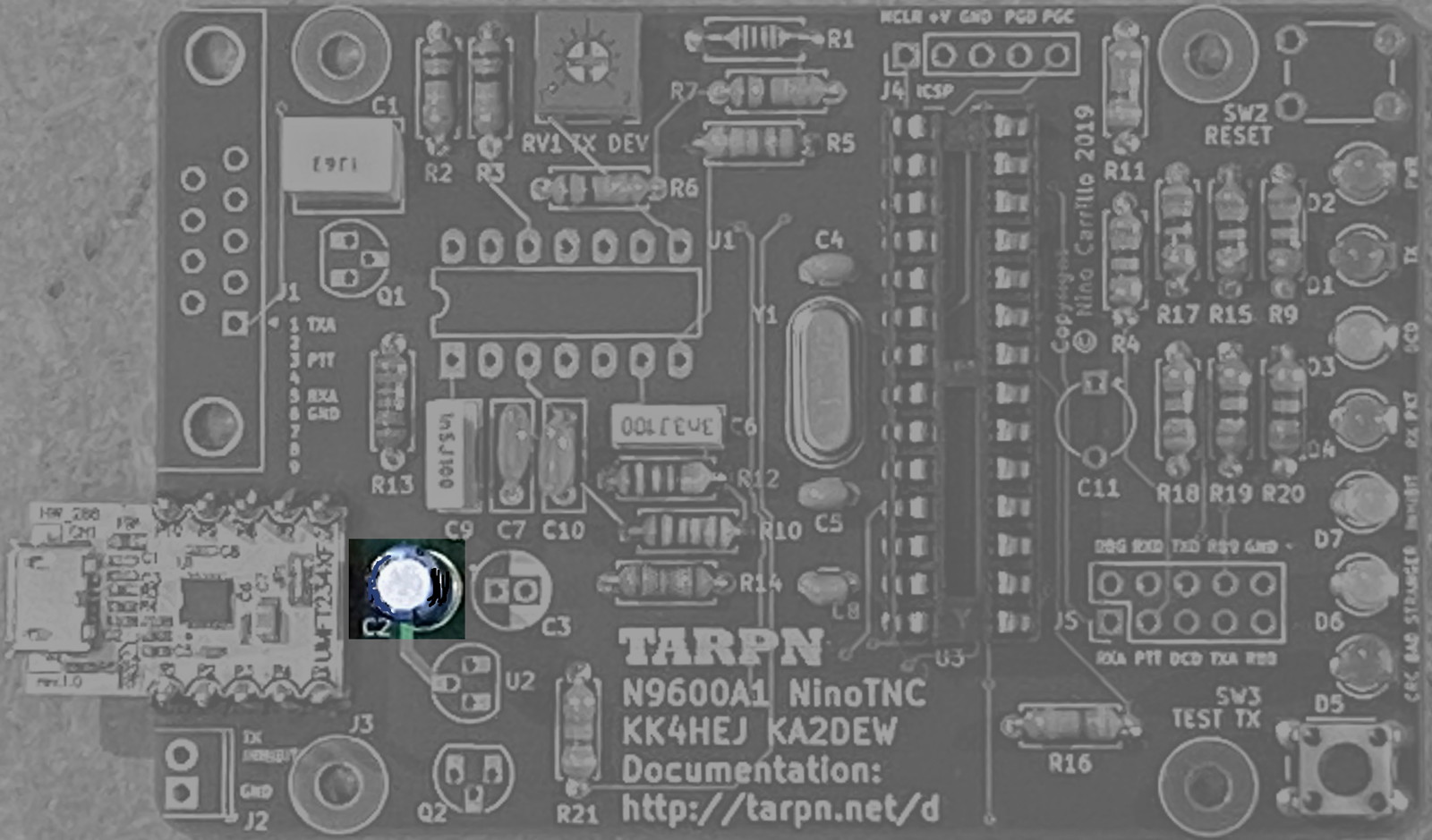 |
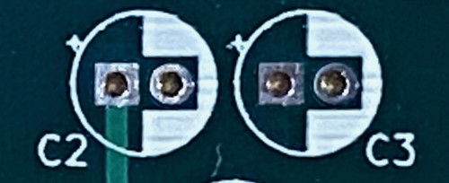
| 26 | C3 | 100uF 10volt aluminum electrolytic capacitor, radial leads 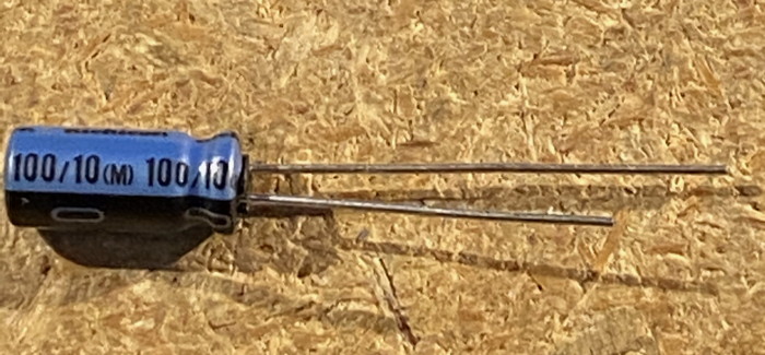 |
Carefully observe values and polarities. Cathode (negative) is marked with a black stripe and go into the round solder pad/hole on the PCB.
The silk-screen actually has a microscopic + sign. Put the --- side away from that.
This is the 3.3v filter capacitor immediately following the regulator.  |
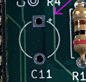
| 27 | C11 | 10 uF Tantalum dipped capacitor radial leads 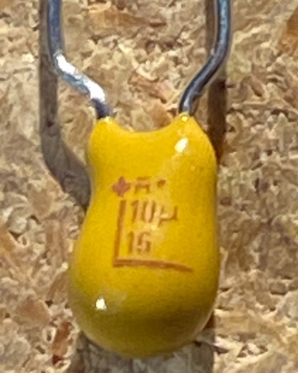 |
This is a polarized component.
It’s solid yellow, round, and larger than the ceramic caps. Marked 10U 16, and it’s polarized. You may need to bend the leads to space them correctly for the pads.
Carefully align the positive lead (marked with “+”) with the square pad (also marked with “+”). The + in both cases are practically microscopic. See pix.
Hooked to the VCAP signal to the CPU, and to ground. 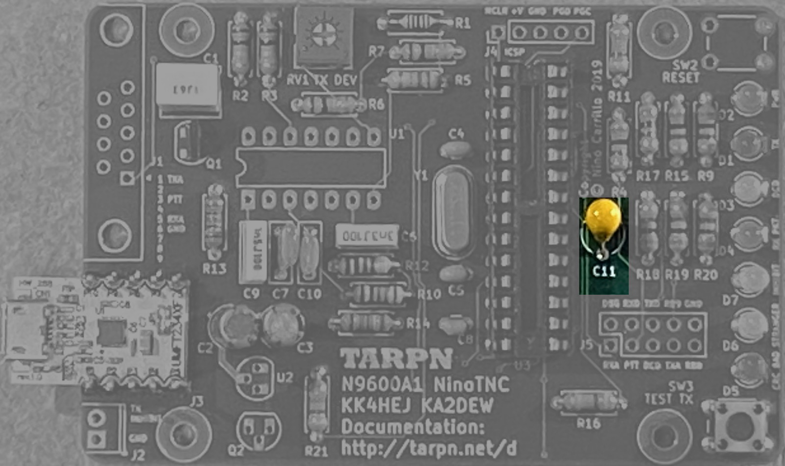
 |
| 28 | Q1 | 2N7000 transistor 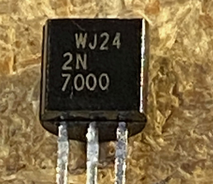 |
Pay attention to the shape of the silkscreen box where this part is inserted.
The flat side of the transistor lines up with the flat side of the silksreen shape.
This transistor is driven by a GPIO on the CPU and is responsible for pulling the PTT line to ground. If this transistor is missing or dead, the TX LED on the TNC will still light, but the radio will not transmit.  |
| 29 | U2 | 1702 Linear Regulator 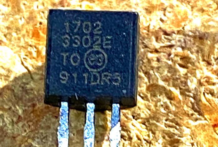 |
This part takes the 5v DC from the USB connector and regulates it down to 3.3v, as needed by the CPU.
 |
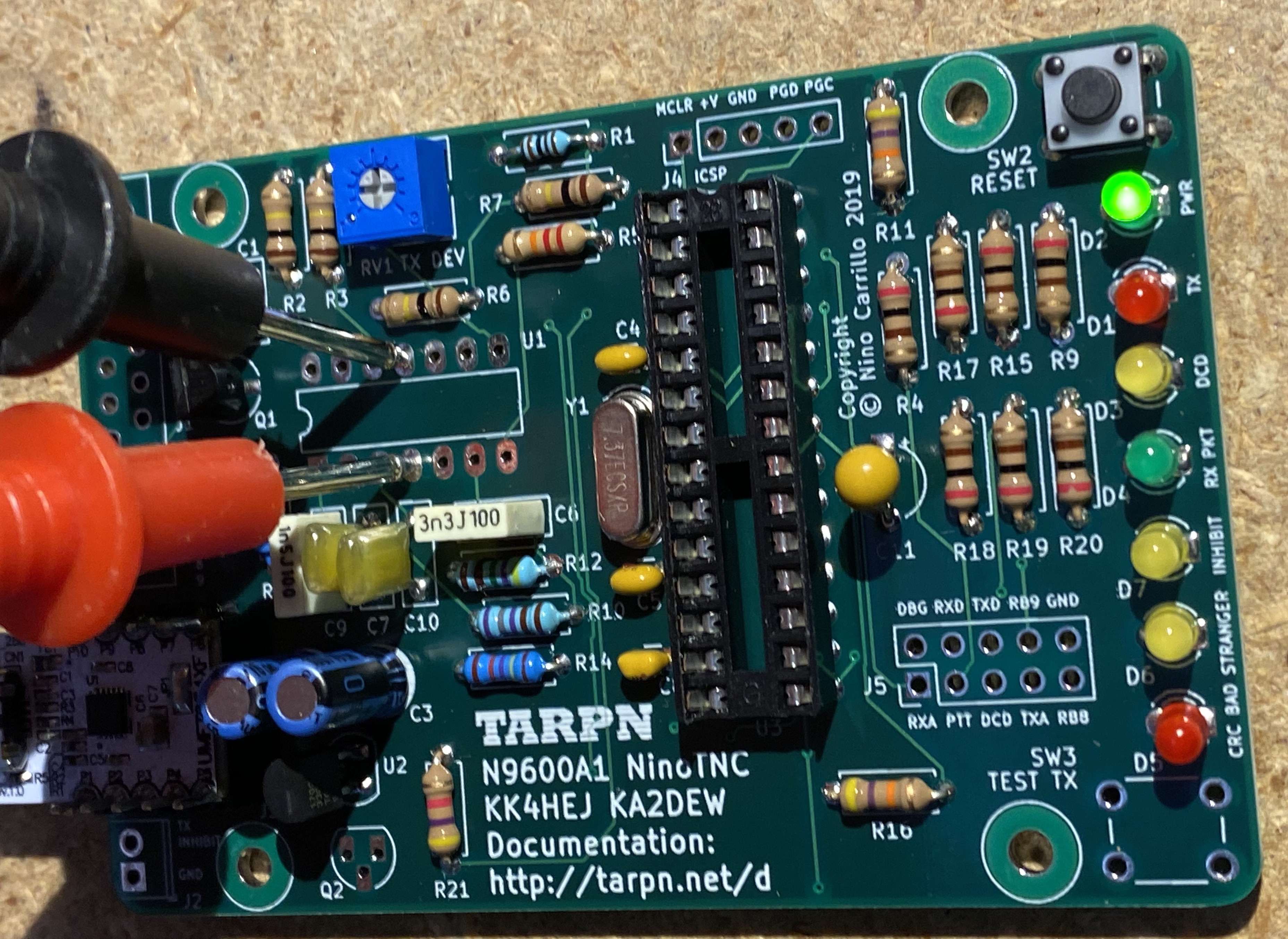
| 30a | U1 | MCP6004 14-pin quad Op-amp package 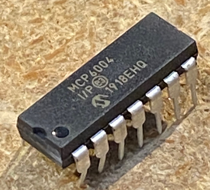
|
Make sure the half-moon shaped end lines up with the PCB as shown in the photos.
Solder only pins 4 and 11 at this time. This is a quad-package op-amp (operational amplifier) used to buffer the receive AF data signal from the radio and to condition and buffer the transmit AF data signal to the radio. 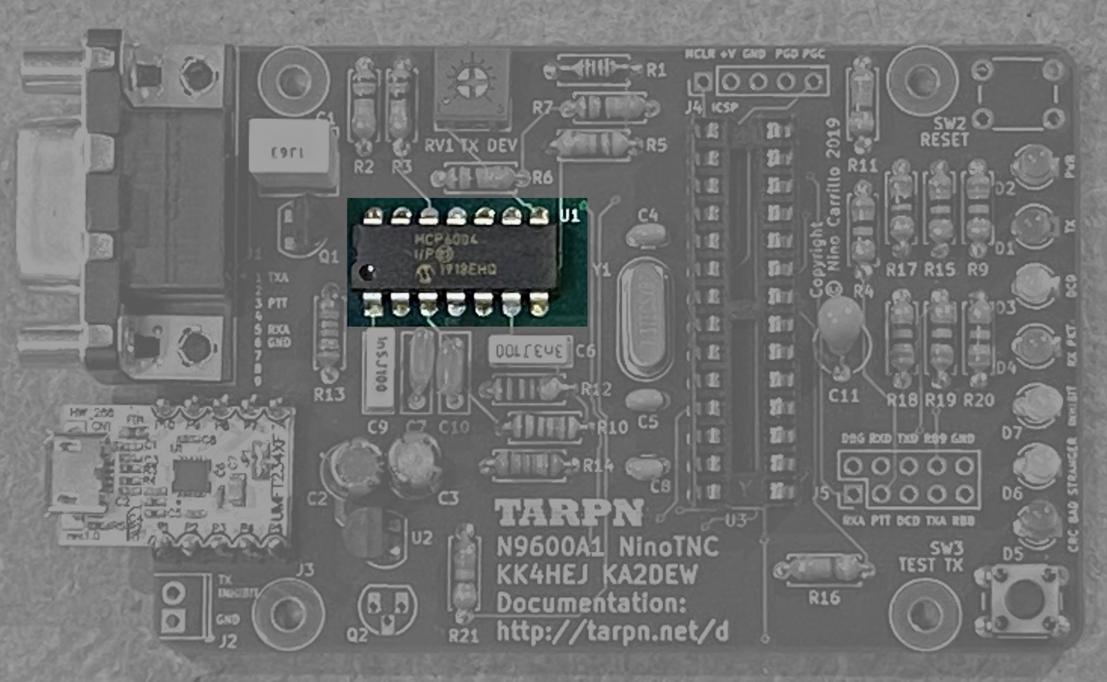 |
| 30b | U1 | MCP6004 14-pin quad Op-amp package |
Finish soldering the remaining 12 pins |
| 31 | J1 | DE9 female connector 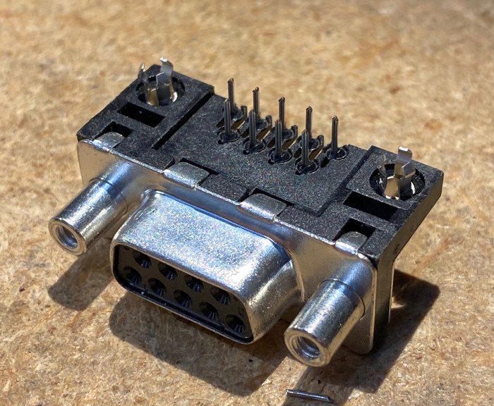 |
This is the interface to the radio.
I recommend inserting the connector (from the top side of the board) and then soldering one of the 9 small pins. Now, squeeze the connector into the board and heat the one pin you soldered. The connector will now fully go flush with the PCB. Once the solder cools, go ahead and solder the other 8 pins, and then finally the 2 large solder pads on the wings to add strength. 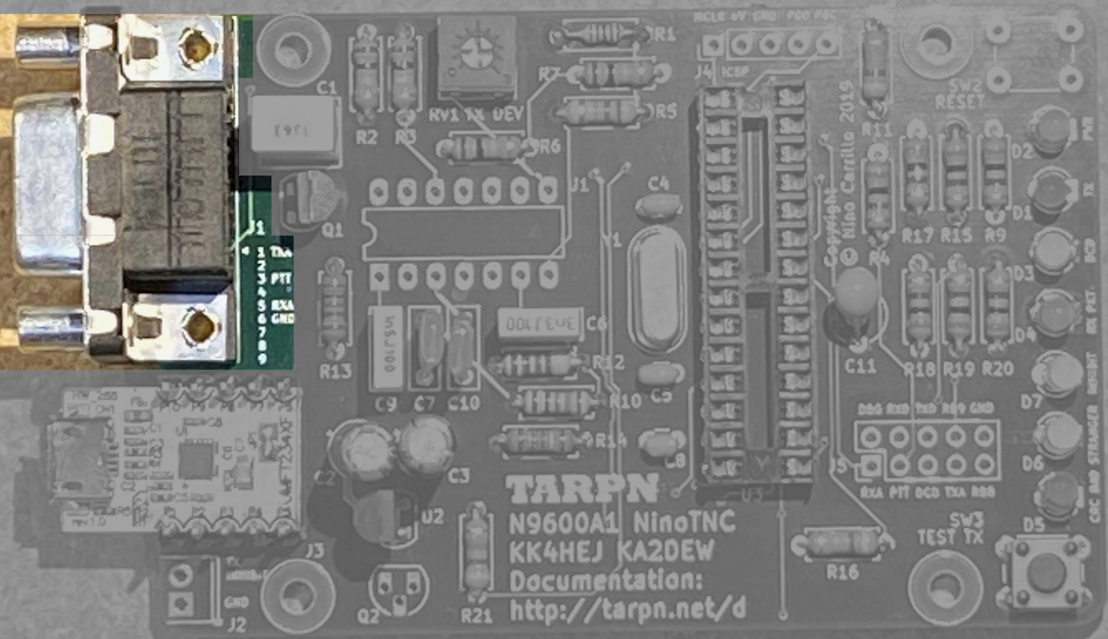 |
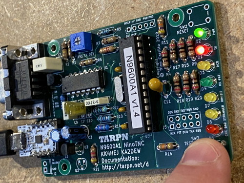
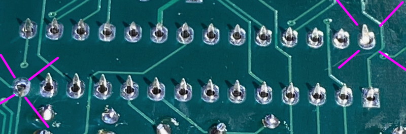
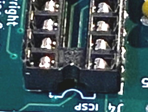
| 32 | U3 | u3 dsPIC 28-pin microprocessor 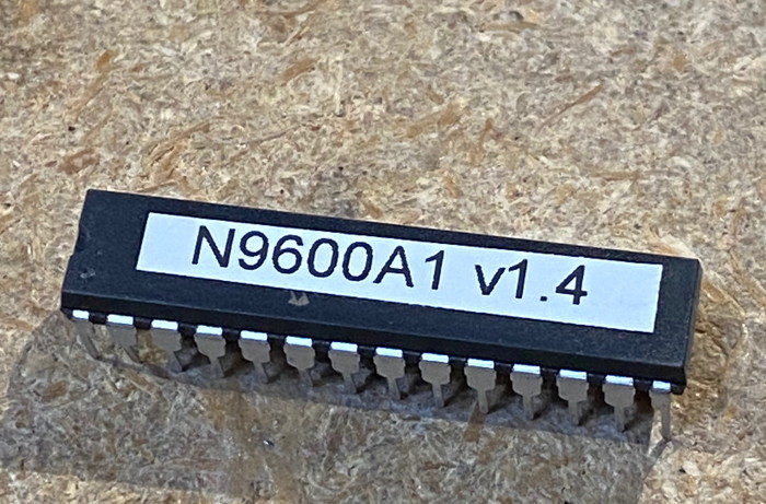
|
Make sure the half-moon shaped end lines up with the PCB as shown in the photos. Watch all of the pins as you insert it the part slowly. Inspect around the chip for bent pins.
 |